
Digital photo induction device

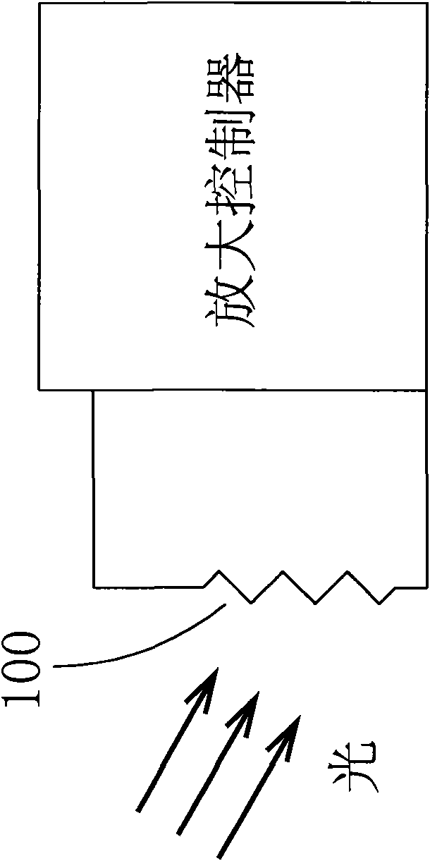
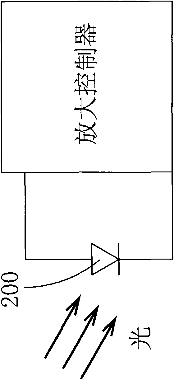
A sensing device and light sensing technology, which is applied in the direction of using electric radiation detectors for light metering, measuring circuits, etc., which can solve the problems of being susceptible to temperature or noise interference, and that a single signal cannot sense two-stage signals.

Inactive Publication Date: 2010-07-14
DIODES INC
View PDF0 Cites 2 Cited by
  • Summary
  • Abstract
  • Description
  • Claims
  • Application Information

AI Technical Summary

Problems solved by technology

[0004] However, if a general light sensor uses the above-mentioned photoresistor 100 or photodiode 200 alone, it is easily disturbed by temperature or noise during operation, and its output only has a single signal and cannot sense two signals; therefore, in order to eliminate the existing defects Problem, the inventor of this case provides a digital light sensing device after several trials and improvements based on his own professionalism and technical concepts and his own experience in this work for many years, which is not easily affected by temperature or It is noise interference, in order to achieve the purpose of accurately detecting the light source, and generate a digital signal output as the light source changes

Method used


Image

  • Digital photo induction device
  • Digital photo induction device
  • Digital photo induction device

Examples


Embodiment Construction

[0013] In order to make it easier for your examiner to understand the content of the present invention and the effects that can be achieved, the detailed descriptions of the accompanying drawings and drawing numbers are as follows:

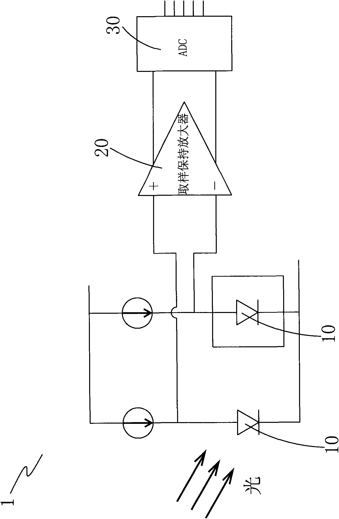
[0014] see image 3 , which is a schematic circuit diagram of the present invention, a digital light sensing device 1, which includes:

[0015] A sampling and holding amplifier (Sampling Hold AMP) 20 is connected to a photosensitive diode 10 at its non-inverting input terminal and inverting input terminal respectively, and then an analog-to-digital converter (ADC) 30 is connected to the output terminal of the sampling and holding amplifier 20 Wherein said photosensitive diode 10 has two, and the P-type connection of a photosensitive diode 10 is connected to the non-inverting input end of the sample-and-hold amplifier 20, and the P-type connection of another photosensitive diode 10 is connected to the sample-and-hold amplifier 20, and the N-type j...


PUM


Abstract

The invention relates to a digital photo induction device, which comprises a sample-and-hold amplifier and an analog-digital converter (ADC). A non-inverting input end and an inverting input end of the sample-and-hold amplifier are respectively connected with a photo induction diode; an output end of the sample-and-hold amplifier is connected with the analog-digital converter (ADC); a digital signal can be output by the analog-digital converter (ADC) to fulfill the aim of detecting a light source; and the output of the digital signal is generated along with the change of the light source.

Description

technical field [0001] The invention relates to a light sensing device, in particular to a digital light sensing device. Background technique [0002] see figure 1 As shown, it is a schematic diagram of a photoresistor. The characteristic of photoresistor 100 is that the resistivity changes with the intensity of incident light. It can respond to light. When there is light, it will conduct electricity immediately; when there is no light, it will stop immediately . [0003] see figure 2 As shown, it is a schematic diagram of a photodiode. The photodiode 200 uses a diode structure. When photons irradiate the depletion region of the diode, the generated electron-hole pairs are separated due to the opposite electric force, and the electron-hole pairs are separated, respectively. Entering the N-type and P-type neutral regions, a photocurrent is formed and the circuit is turned on. [0004] However, if a general light sensor uses the above-mentioned photoresistor 100 or photod...

Claims


Application Information

Patent Timeline
IPC IPC(8): G01J1/44
Inventor 李明辉黄照昌纪全鸿
Owner DIODES INC
Learn More