Embedded capacitance printed circuit board and production method thereof

A technology for printed circuit boards and manufacturing methods, which is applied in the manufacture of printed circuits, assembly of printed circuits with electrical components, printed circuits, etc., and can solve problems such as tearing of inner layer boards, easy slippage of inner layer boards, and lower product yields , to achieve the effect of improving strength, ensuring no slippage, and improving product yield

Inactive Publication Date: 2010-07-07
GCI SCI & TECH
View PDF2 Cites 5 Cited by
  • Summary
  • Abstract
  • Description
  • Claims
  • Application Information

AI Technical Summary

Problems solved by technology

Because the board is too thin, it is easy to slip between the inner boards during the pressing operation, resulting in open and short circuit of the inner layer graphic circuit or deviation of capacitance value, and even defects such as tearing and damage of the inner board, making Product yield is low
[0004] In conventional printed circuit boards, in order to prevent the flow of glue during the lamination process of the multi-layer board core, the frame of each layer of the inner layer of the board is often designed with a flow blocking block. If the layer board is too thin, the block design of the frame of the inner layer board will further weaken the supporting force of the inner layer graphics, and even cause the graphics to tear, further reducing the product yield

Method used


Image

  • Embedded capacitance printed circuit board and production method thereof
  • Embedded capacitance printed circuit board and production method thereof
  • Embedded capacitance printed circuit board and production method thereof

Examples


Embodiment approach 1

[0023] This implementation mode is a specific implementation mode of the first technical solution of the present invention.

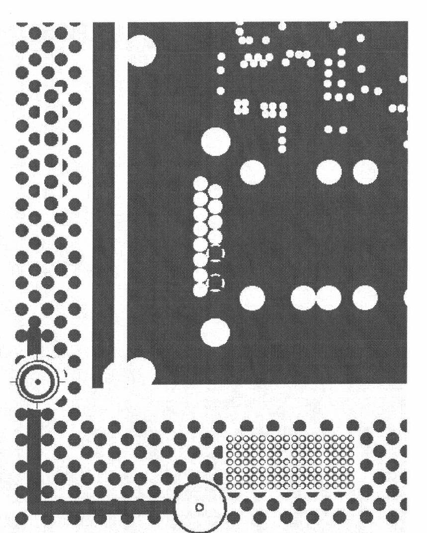
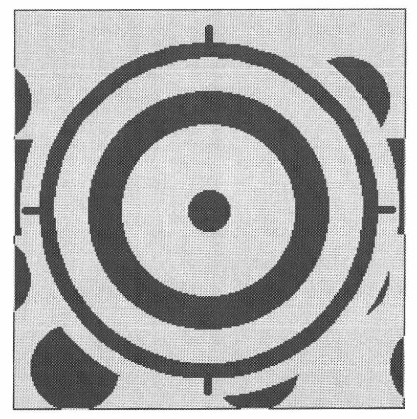
[0024] The embedded capacitor printed circuit board of this embodiment includes multilayer boards for forming capacitors, each layer of boards includes a thin film material layer and copper layers covering both sides of the thin film material layer. figure 1 It is a partial view of a layer of the existing printed circuit board, and its frame part is provided with a blocking block for blocking and controlling the flow of glue in the pressing process, such as figure 2 As shown, in the board frame of the present invention, the blocking block part is set as several evenly distributed glue flow grooves 1, and the glue flow grooves are only arranged in the copper layers on both sides of the board. . Because the design of the flow glue tank of the present invention retains most of the copper layer on the surface of the original board, the frame strength of t...


PUM


Abstract

The invention discloses an embedded capacitance printed circuit board, which comprises multiple layers of sheet for forming capacitance, wherein each layer of sheet comprises a film material layer and a layer covered on both sides of the film material layer. The embedded capacitance printed circuit board is characterized in that: flowed glue grooves used for flowed glue are distributed on borders on both sides of the sheet, and the flowed glue grooves are arranged in the copper layer on both sides of the sheet. Due to the long and thin flowed glue grooves in uniform distribution produced on the copper layer of the borders on both sides of the sheet, the problem of the flowed glue in the process of laminating a sheet chip is solved, the strength of the frame of each layer of inner sheet can be improved, and the defects of pattern tearing and the like are unlikely to occur. In addition, the invention also discloses a method for producing the embedded capacitance printed circuit board.

Description

technical field [0001] The invention relates to a printed circuit board, in particular to an embedded capacitor printed circuit board and a manufacturing method thereof. Background technique [0002] Electronic products are gradually developing in the direction of refinement and high density, especially for high-end special industry products. With the increase in the number of electronic components installed on the surface of printed circuit boards, it is difficult to mount electronic components on the surface. Therefore, embedded type technology. The benefits of placing capacitive components inside the board go beyond saving space on the board surface. The welding points on the surface of the circuit board will generate inductance, and the embedding method eliminates the welding points, thereby reducing the introduced inductance, thereby reducing the impedance of the power system. As a result, the embedded process saves valuable board surface space, reduces board size, an...

Claims


Application Information

Patent Timeline
Patent Type & Authority Applications(China)
IPC IPC(8): H05K1/16H05K3/00H05K3/30
Inventor 任代学王晓伟黄德业
Owner GCI SCI & TECH
Why Eureka
Try Eureka