Method for flattening film layer

A planarization and film layer technology, applied in the field of planarization, can solve the problems of good and bad connection pad quality, affecting thickness uniformity, etc.

Inactive Publication Date: 2012-07-04
UNIMICRON TECH CORP
View PDF0 Cites 0 Cited by
  • Summary
  • Abstract
  • Description
  • Claims
  • Application Information

AI Technical Summary

Problems solved by technology

In addition, this poorly flat solder mask affects its thickness uniformity and the quality of the solder pads connected to external electronic parts

Method used


Image

  • Method for flattening film layer
  • Method for flattening film layer
  • Method for flattening film layer

Examples


Embodiment Construction

[0030] In order to make the above and other objects, features and advantages of the present invention more comprehensible, the following specific embodiments are described in detail together with the accompanying drawings.

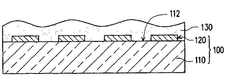
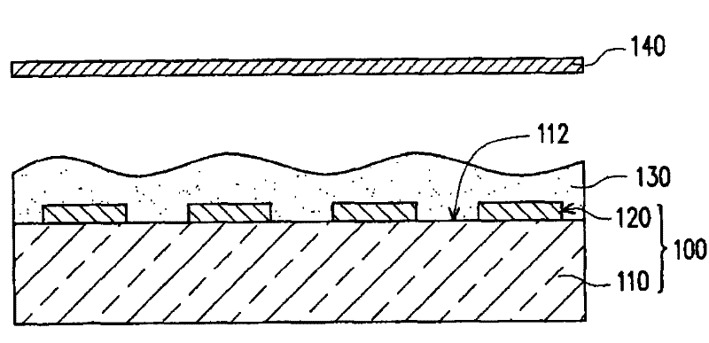
[0031] Figure 1A to Figure 1F It is a schematic cross-sectional view of a method for flattening a film layer according to an embodiment of the present invention. Please refer to Figure 1A Regarding the film planarization method of this embodiment, firstly, a circuit board 100 is provided. The circuit board 100 has a dielectric layer 110 and a patterned circuit layer 120 , wherein the dielectric layer 110 has a surface 112 , and the patterned circuit layer 120 is located on the surface 112 of the dielectric layer 110 .

[0032] It is worth mentioning that the structure of the circuit board 100 may have only one patterned circuit layer 120 , or may have multiple patterned circuit layers. That is, the circuit board 100 may be a single side circuit board, ...


PUM

PropertyMeasurementUnit
hardnessaaaaaaaaaa

Abstract

The present invention relates to a method for flattening a film layer. Firstly, a circuit board is provided. The circuit board is provided with a dielectric layer and a patterned circuit layer, wherein the dielectric layer has a surface, and the patterned circuit layer is arranged on the surface. A film layer is subsequently formed on the circuit board, and the surface of the dielectric layer andthe patterned circuit layer are covered by the film layer. A release film is arranged on the film layer. Then, the release film is tightly pressed to the film layer by a first hot pressing technique.

Description

technical field [0001] The present invention relates to a method for planarization, and in particular to a method for planarizing a film layer by using a pressing process. Background technique [0002] With the rapid development of the digital industry, the application of circuit boards in digital products is becoming more and more extensive. For example, there are circuit boards in mobile phones, computers, digital cameras and other products, and the main function of circuit boards is to carry external Electronic components, and then achieve the purpose of electrical conduction. [0003] Generally speaking, after the circuit layer on the circuit board is completed, a polymer material layer will be formed on the circuit board to cover part of the circuit layer and expose multiple solder pads of the circuit layer, and then the external electronic The parts are connected to the solder pads, and the polymer material layer used for this protection is the solder mask. [0004] ...

Claims


Application Information

Patent Timeline
Patent Type & Authority Patents(China)
IPC IPC(8): H05K3/28G03F7/20G03F7/30
Inventor 刘逸群王定中李永浚宋尚霖陈宗源陈国庆
Owner UNIMICRON TECH CORP
Why Eureka
Try Eureka