Processor Cache write-in invalidation processing method based on memory access history learning
A processing method and processor technology, applied in memory systems, electrical digital data processing, instruments, etc., can solve problems such as difficult and efficient support of memory access characteristics in write allocation strategies, and achieve the effect of improving performance and reducing bandwidth waste
- Summary
- Abstract
- Description
- Claims
- Application Information
AI Technical Summary
Problems solved by technology
Method used
Image
Examples
example 1
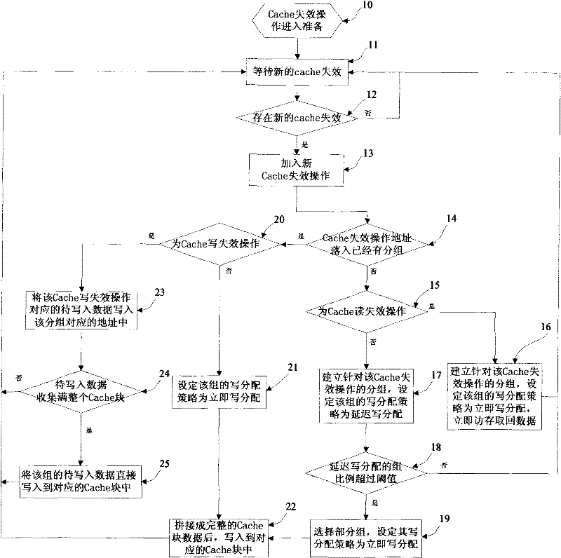
[0086] Example 1. Assume that the memory access invalidation queue has the following three items, among which item 0 and item 1 are valid, and their addresses are 0x0401000 and 0x001f00c0 respectively. Item 0 of the two items is delayed write allocation, and item 1 is immediate write allocation. . Among them, 16 bytes of data from 0x0401000 to 0x0401000f have been stored in item 0. Then the addresses of the four words and operations entering the memory access unit are 0x0401001c, 0x04010010, 0x04010014, 0x04010018 respectively. These four operations will miss the cache and enter the memory access invalidation queue. After address comparison, these four operations all fall within the range of item 0 of the queue, so these four operations also inherit the delayed write allocation of item 0. The memory read request is delayed until the fourth write operation also enters the memory access invalidation queue. At this point, item 0 has collected the entire cache block, so there is ...
example 2
[0087] Example 2. Assume that there are 3 items in the memory access invalidation queue, of which item 0 and item 2 are valid, and their addresses are 0x04000000 and 0x007f0040 respectively. The second item in the two items is delayed write allocation, the delay field is set to 1, and item 0 For immediate write allocation, that is, the delay field is set to 0. At this time, a byte write operation with an address of 0x007f00c8 enters the memory access unit. After searching, it misses in the Cache, so it needs to enter the memory access invalidation queue. By comparing the addresses with the existing two items in the memory access queue, the new write failure does not fall into any of the items, so a new item is assigned to it in the memory access invalidation queue. Therefore, the first item is valid, the address field is set to 0x007f00c0, the 64 to 71 bits of the data field store the value to be written in the write operation, and the eighth bit of the mask byte mask field is...
example 3
[0088] Example 3. Assume that there are 3 items in the memory access invalidation queue, of which item 0 and item 2 are valid, and their addresses are 0x04000000 and 0x007f0040 respectively. Item 2 of the two items is delayed write allocation, and item 0 is immediate write allocation. Only one word of data at address 0x0400000c is stored in item 2. At this time, a byte read operation whose address is 0x04000004 enters the memory access unit, and it misses in the Cache after searching, so it needs to enter the memory access invalidation queue. By comparing the address with the existing two items in the memory access queue, it is judged that it falls in item 0, but after further searching, it is found that the required data is not currently in the data field, so the delay field of item 0 is set to 0 , immediately initiate a memory read access.
PUM
 Abstract
Description
Claims
Application Information
 - R&D
- Intellectual Property
- Life Sciences
- Materials
- Tech Scout
- Unparalleled Data Quality
- Higher Quality Content
- 60% Fewer Hallucinations
Browse by: Latest US Patents, China's latest patents, Technical Efficacy Thesaurus, Application Domain, Technology Topic, Popular Technical Reports.
© 2025 PatSnap. All rights reserved.Legal|Privacy policy|Modern Slavery Act Transparency Statement|Sitemap|About US| Contact US: help@patsnap.com


