Spin-polarized charge carrier device
A technology of spin polarization and carrier, applied in the field of polarimeter
- Summary
- Abstract
- Description
- Claims
- Application Information
AI Technical Summary
Problems solved by technology
Method used
Image
Examples
Embodiment Construction
[0043] Device structure
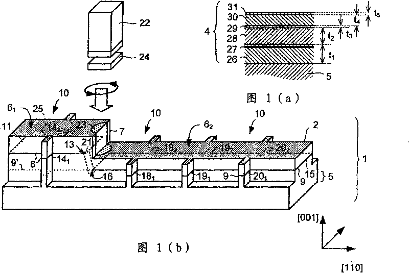
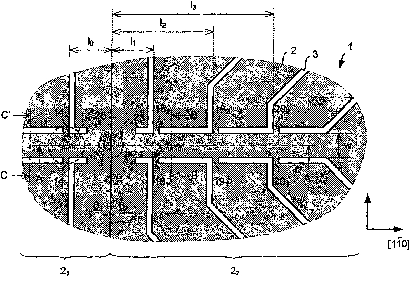
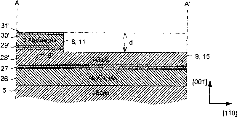
[0044] refer to Figure 1(b) , 1(a) and 2 to 5, show an electro-optic, spin-polarized carrier device. The device 1 comprises mesas 2 defined by trench isolation by using etched trenches 3 . The mesas 2 are used to pattern an aluminum gallium arsenide / gallium arsenide (AlGaAs / GaAs) heterostructure 4 on an undoped GaAs substrate 5 ( FIG. 1( a )). The mesa 2 is stepped with an upper unetched plane 6 1 and lower etch plane 6 2 . Thus, the mesa 2 is divided into a first and a second part 2 along the step edge 7 1 ,2 2 . Laddering the mesa 2 so that in the first part 2 of the mesa 2 1 Form two-dimensional hole gas (2DHG) 8 and the second part 2 of the mesa 2 2 A two-dimensional electron gas (2DEG) is formed9.
[0045] 2DEG 9 aggregates have sheet concentration n 2DEG =2.5×10 11 and mobility μ=3×10 3 cm 2 / Vs electrons. However, part 9' of 2DHG located below 2DHG 8 is depleted.
[0046] The mesa 2 comprises a hall bar structure 10 spanning th...
PUM
| Property | Measurement | Unit |
|---|---|---|
| thickness | aaaaa | aaaaa |
| thickness | aaaaa | aaaaa |
Abstract
Description
Claims
Application Information
 - R&D Engineer
- R&D Manager
- IP Professional
- Industry Leading Data Capabilities
- Powerful AI technology
- Patent DNA Extraction
Browse by: Latest US Patents, China's latest patents, Technical Efficacy Thesaurus, Application Domain, Technology Topic, Popular Technical Reports.
© 2024 PatSnap. All rights reserved.Legal|Privacy policy|Modern Slavery Act Transparency Statement|Sitemap|About US| Contact US: help@patsnap.com


