


Quick Research
Generate reliable direction feasibility study reports for your R&D in just a few steps.

Technical Q&A
Discover and master advanced knowledge NOW. Basics, ideas, possibilities, all at once.

Find Solutions
As an expert in R&D theories, this can generate solutions to your technical problems instantly.

Evaluate Feasibility
Analyze your overall solution with one click, know your potential R&D risks in advance.

Monitor Landscape
Get weekly tech updates, stay abreast of the latest tech innovations and key insights.
Filter circuit and voltage-controlled oscillating circuit
A filter circuit and branch circuit technology, which is applied in the field of voltage-controlled oscillation circuits, can solve the problems that useless signals cannot be fully offset.
- Summary
- Abstract
- Description
- Claims
- Application Information
AI Technical Summary
Problems solved by technology
Method used
Image

Examples
Deformed example 1
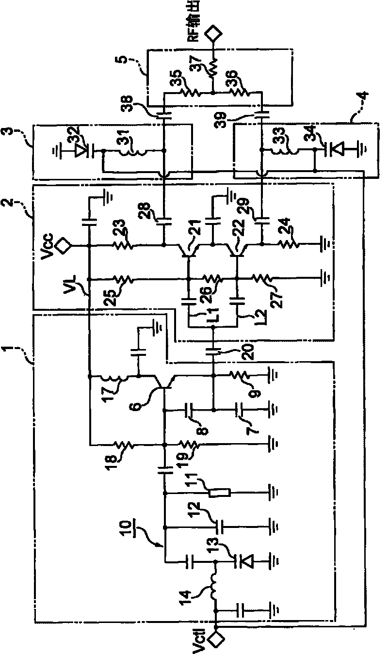
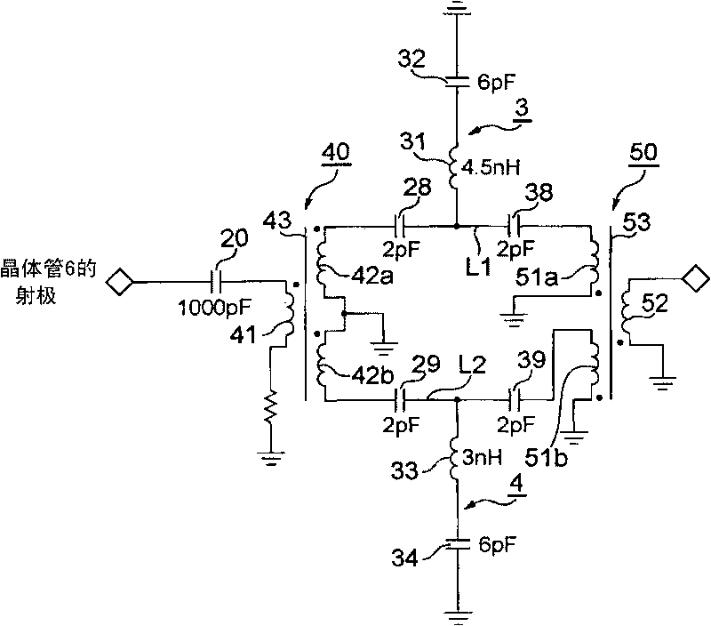
[0047] figure 2 is true figure 1 A configuration diagram of Modification 1 in which the circuit configuration after the oscillator circuit section 1 in the shown voltage controlled oscillator is modified. The notch circuit has the same structure as the above-mentioned embodiment. The oscillation circuit unit 1 is omitted from illustration.
[0048] Modification 1: The high-frequency transformer directional coupler 40 that simultaneously performs wave splitting and phase inversion as the output splitter circuit 2 is provided at the front end of the filter section, and the high-frequency transformer coupler 50 as the output resynthesis circuit 5 is provided at the front end of the filter section. The rear section of the filter section.
[0049] The high-frequency transformer splitter 40 has a primary side coil 41, secondary side coils 42a, 42b, and an iron core 43. One end of the primary side coil 41 is connected to the emitter of the oscillating transistor 6, and the other ...
Deformed example 2
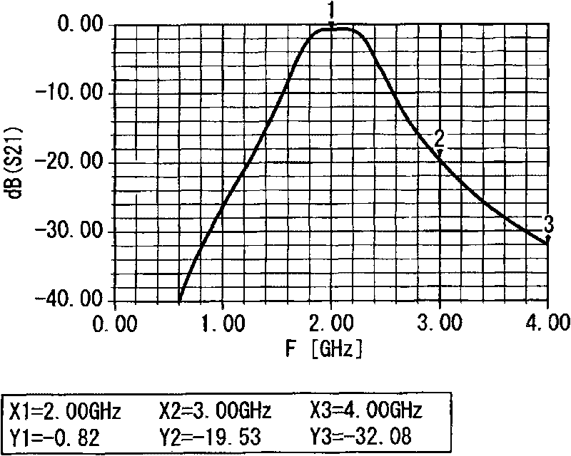
[0054] Figure 4 is said to be figure 2 A configuration diagram of Modification 2 in which the trap circuit in the shown circuit configuration is replaced by an LC parallel circuit. The trap circuit 60 is constituted by a parallel resonance circuit of an inductor 61 and a capacitor 62 . The trap circuit 70 has the same structure as the trap circuit 60 and is composed of a parallel resonance circuit of an inductor 71 and a capacitor 72 .
[0055] Such as Figure 4 As shown, the inductance value of the trap circuit 60 is set to 1.0nH, the capacity is set to 24pF, and the notch frequency is set to 1.03GHz with respect to the oscillation frequency of 1.0GHz. Furthermore, the inductance value of the trap circuit 70 was set to 1.0 nH, the capacitance was set to 27 pF, and the trap frequency was set to 0.97 GHz.
[0056] Figure 5 is based on Figure 4 The circuit model is shown along with the attached diagram of the results of simulating the filter characteristics with circuit ...
Deformed example 3
[0058] Figure 6 It is a structural diagram of Modification 3. Modification 3 combines an output demultiplexing circuit 2, a trap circuit 3, a trap circuit 4, and a high-frequency transformer coupler 50. The output demultiplexing circuit 2 uses a series connection of transistors Inverting the phase, the above-mentioned trap circuit 3 and trap circuit 4 are constituted by LC series resonant circuits.
[0059] In the notch circuit 3, a notch frequency (fo-Δ) shifted slightly to the low-band side with respect to the oscillation frequency (fo=2.0 GHz) is set. In addition, in the notch circuit 4 , a notch frequency (fo+Δ) shifted slightly to the high frequency band side is set.
[0060] Figure 7 is based on Figure 6 Figure 1. Results of simulated filtering characteristics of the circuit model shown. From the simulation results, it can be seen that steep filter characteristics are realized.
PUM
 Abstract
Description
Claims
Application Information
 - R&D Engineer
- R&D Manager
- IP Professional
- Industry Leading Data Capabilities
- Powerful AI technology
- Patent DNA Extraction
Browse by: Latest US Patents, China's latest patents, Technical Efficacy Thesaurus, Application Domain, Technology Topic, Popular Technical Reports.
© 2024 PatSnap. All rights reserved.Legal|Privacy policy|Modern Slavery Act Transparency Statement|Sitemap|About US| Contact US: help@patsnap.com