
Level shifter circuit incorporating transistor snap-back protection

A technology of level shifter and voltage shift, which is applied in the direction of logic circuit coupling/interface, logic circuit, logic circuit connection/interface arrangement using field effect transistors, etc., which can solve the problem that level shifter circuits cannot be used.

Active Publication Date: 2010-03-24
SANDISK TECH LLC
View PDF1 Cites 12 Cited by
  • Summary
  • Abstract
  • Description
  • Claims
  • Application Information

AI Technical Summary

Problems solved by technology

As a result, standard size level shifter circuits cannot be used for varying output capacitive loads without incurring a reliability risk to the level shifter circuit

Method used


Image

  • Level shifter circuit incorporating transistor snap-back protection
  • Level shifter circuit incorporating transistor snap-back protection
  • Level shifter circuit incorporating transistor snap-back protection

Examples


Embodiment Construction

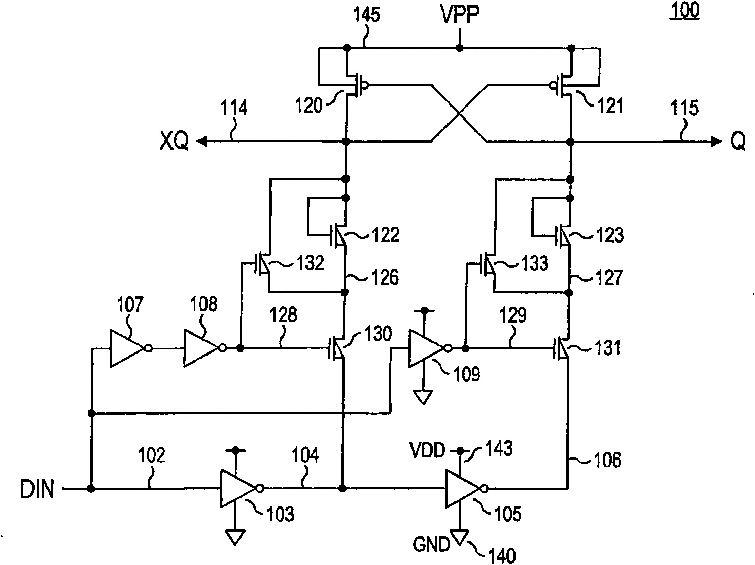
[0027] now refer to figure 2 , shows a level-shifting circuit that does not require intentional weakening of the pull-down path and that is protected from the jump-through effect regardless of the output load. As before, logic signal DIN is transmitted on node 102 and inverted by low voltage inverter 103 to generate a VDD level control signal at node 104 which is inverted by low voltage inverter 105 phase to generate a VDD level control signal at node 106 . The inverters 103, 105 can be regarded as belonging to the VDD voltage range (ie, the low voltage range), and the input signal DIN transmitted on the node 102 and the control signals transmitted on the nodes 104, 106 can be regarded as having a voltage corresponding to VDD and VDD respectively. The high level and low level VDD range (that is, low voltage range) signals corresponding to the ground.

[0028] Complementary XQ, Q output nodes 114, 115 are coupled to VPP through cross-coupled PMOS transistors 120, 121 and to g...


PUM


Abstract

Level shift circuits are disclosed for level shifting an input signal corresponding to a first voltage domain, to generate a pair of complementary output signals corresponding to a second, higher-voltage domain. Snap-back sensitive devices in a discharge circuit for a high voltage output node are protected, irrespective of the loading on the output node, and without requiring precise transistor sizing as a function of the output loading. The snap-back sensitive devices are protected by a voltage shifter circuit in series with the sensitive devices, to limit the voltage across the sensitive devices, even for a high capacitance output node at its highest output voltage. The voltage shifter circuit is then bypassed to provide for an output low level that fully reaches the lower power supply rail.

Description

technical field [0001] The present invention relates to a level shifting circuit for generating a high voltage domain output signal in response to a low voltage domain input signal. Background technique [0002] Level shifting circuits are commonly used to shift signals from a low voltage range to a high voltage range. For example, logic signals may be generated by circuits powered by a low supply voltage such as VDD (eg, 1.5 volts), and thus typically have output levels corresponding to VDD and ground. However, many circuits, such as programmable memory devices, utilize higher voltages for internal signals in program and erase modes than in read mode. Typically, such devices use an internal supply voltage of 3-10 volts or higher, which may be referred to as VPP. Thus, it is useful to generate level-shifted "versions" of these low-level logic signals to provide appropriate voltages at various switching circuit nodes, especially during the program and erase modes of operati...

Claims


Application Information

Patent Timeline
Patent Type & Authority Applications(China)
IPC IPC(8): H03K19/0185
CPCH03K3/35613H03K17/102H03K19/01721H03K19/0185
Inventor 泰勒·J·索普卢卡·G·法索利
Owner SANDISK TECH LLC
Learn More