A semiconductor device package using discrete conductive layer to re-select bonding line path
A technology of conductive lines and conductive paths, which is applied in the direction of semiconductor devices, semiconductor/solid-state device manufacturing, semiconductor/solid-state device components, etc., and can solve problems such as unrealistic replacement
- Summary
- Abstract
- Description
- Claims
- Application Information
AI Technical Summary
Problems solved by technology
Method used
Image
Examples
Embodiment Construction
[0058] While the following detailed description contains many specific details for purposes of illustration, those of ordinary skill in the art will appreciate that many changes and substitutions to the following details are within the scope of the invention. Accordingly, the embodiments of the present invention described below are without loss of generality and do not place limitations on the claims of the present invention.
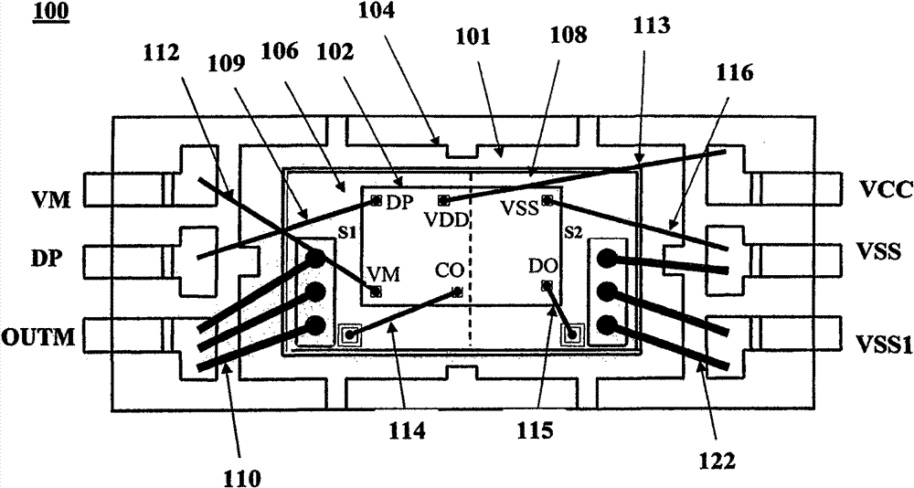
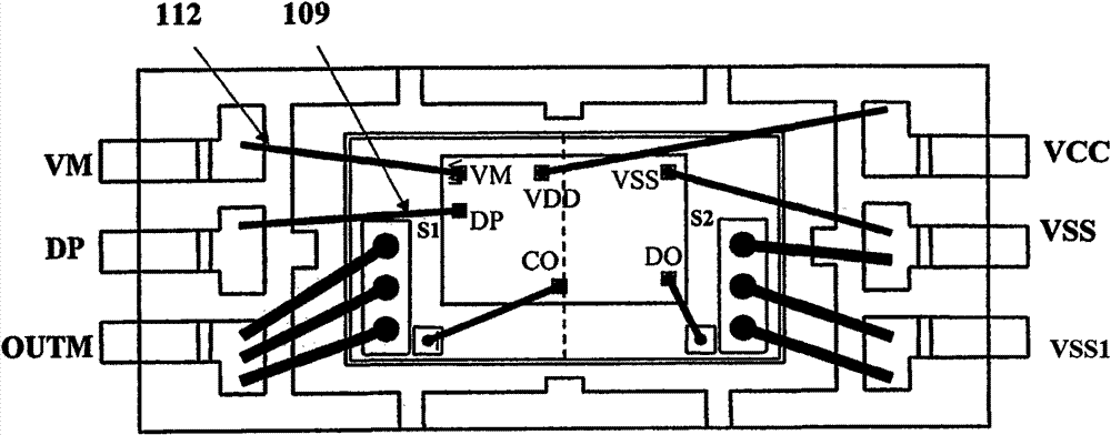
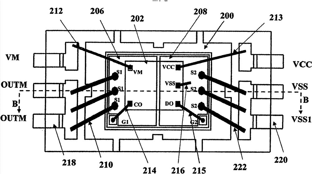
[0059] Embodiments of the present invention overcome the above-mentioned problems by using a semiconductor device that includes electrically isolated conductive traces formed on a layer of conductive material located on top of the device. A conductive trace is configured to provide a conductive path between the first bond wire and the second bond wire. The conductive path is located under the third bonding wire, thus avoiding the situation where the third bonding wire crosses the other bonding wire. The bonding wires that would cross the third bonding ...
PUM
 Abstract
Description
Claims
Application Information
 - R&D
- Intellectual Property
- Life Sciences
- Materials
- Tech Scout
- Unparalleled Data Quality
- Higher Quality Content
- 60% Fewer Hallucinations
Browse by: Latest US Patents, China's latest patents, Technical Efficacy Thesaurus, Application Domain, Technology Topic, Popular Technical Reports.
© 2025 PatSnap. All rights reserved.Legal|Privacy policy|Modern Slavery Act Transparency Statement|Sitemap|About US| Contact US: help@patsnap.com


