
Image sensor and manufacturing method thereof

A photodetector and color filter array technology, which is applied in semiconductor/solid-state device manufacturing, electric solid-state devices, semiconductor devices, etc., to achieve the effects of improving sensitivity, reducing noise, and reducing interference effects

Inactive Publication Date: 2010-03-10
DONGBU HITEK CO LTD
View PDF5 Cites 1 Cited by
  • Summary
  • Abstract
  • Description
  • Claims
  • Application Information

AI Technical Summary

Problems solved by technology

However, since the photodetector can only be formed in an area outside the logic circuit, the area used as the logic circuit limits the area of ​​the photodetector

Method used


Image

  • Image sensor and manufacturing method thereof
  • Image sensor and manufacturing method thereof
  • Image sensor and manufacturing method thereof

Examples


Embodiment Construction

[0023] Hereinafter, the present invention will be described in detail with reference to the accompanying drawings that form a part of this application.

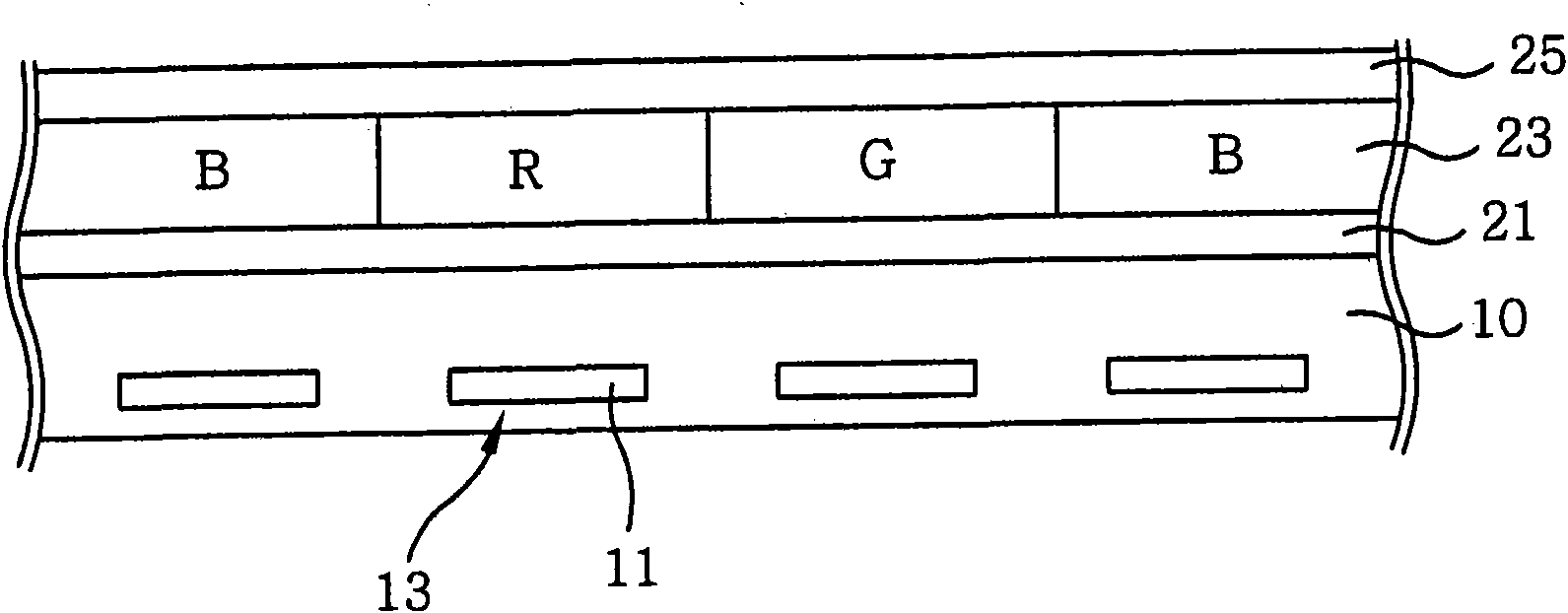
[0024] figure 2 is a cross-sectional view of an image sensor formed by using an image sensor manufacturing method according to an embodiment of the present invention. refer to figure 2 , the image sensor of the embodiment of the present invention may include: a semiconductor substrate 100 having a photodetector 104 and a color filter array 108; a planarization layer 110 having a stepped portion, wherein the stepped portion corresponds to a first group of micro The area of ​​the lens 112 and the area where the second set of microlenses 116 may be formed; the first set of microlenses 112 and the second set of microlenses 116 . The first set of microlenses 112 has a hydrophilic surface characteristic, while the second set of microlenses 116 has a hydrophobic surface characteristic. In addition, reference numeral 102 denotes...


PUM


Abstract

An image sensor has a large bridge margin from a repulsive force between adjacent micro lenses having different surface properties. The image sensor has a larger bridge margin with a configuration ofa stepped portion between two areas, where the first and the second group of micro lenses are formed, over a planarization layer below these two areas. Thus, a zero gap is realized, where no gap between micro lenses exists, and the fill factor of micro lens is maximized. By the realization of the zero gap, interference effects decrease, noise decreases, and fill factor increases, and thus the sensitivity of an image sensor increases, especially the green sensitivity.

Description

technical field [0001] The present invention relates to an image sensor and a manufacturing method thereof, and more particularly, to an image sensor having adjacent microlenses having different surface properties and a manufacturing method thereof. Background technique [0002] An image sensor is a semiconductor device that converts an optical image into an electrical signal. Types of image sensors include CCD (Charge Coupled Device) image sensors and CMOS (Complementary Metal Oxide Semiconductor) image sensors. [0003] A CMOS image sensor is a device that converts an optical image into an electrical signal using CMOS manufacturing technology. CMOS sensors employ a switching method that makes as many MOS transistors as there are pixels and uses them to sequentially detect output. CMOS image sensors are easier to handle than CCD image sensors, have a flexible scanning method, and reduce the size of final products by integrating image detection and signal processing circui...

Claims


Application Information

Patent Timeline
Patent Type & Authority Applications(China)
IPC IPC(8): H01L27/146H01L31/0232H01L21/822H01L31/18
CPCH01L27/14685H01L27/14627H01L27/146
Inventor 朴珍皞
Owner DONGBU HITEK CO LTD
Learn More