Semiconductor device
A semiconductor and conductive technology, applied in the direction of semiconductor devices, transistors, electric solid devices, etc., can solve the problems of poor adhesion, poor wettability, and height difference of metal sheets 131, so as to suppress poor wettability and prevent Smaller size and lower resistance effect
- Summary
- Abstract
- Description
- Claims
- Application Information
AI Technical Summary
Problems solved by technology
Method used
Image

Examples
Embodiment Construction
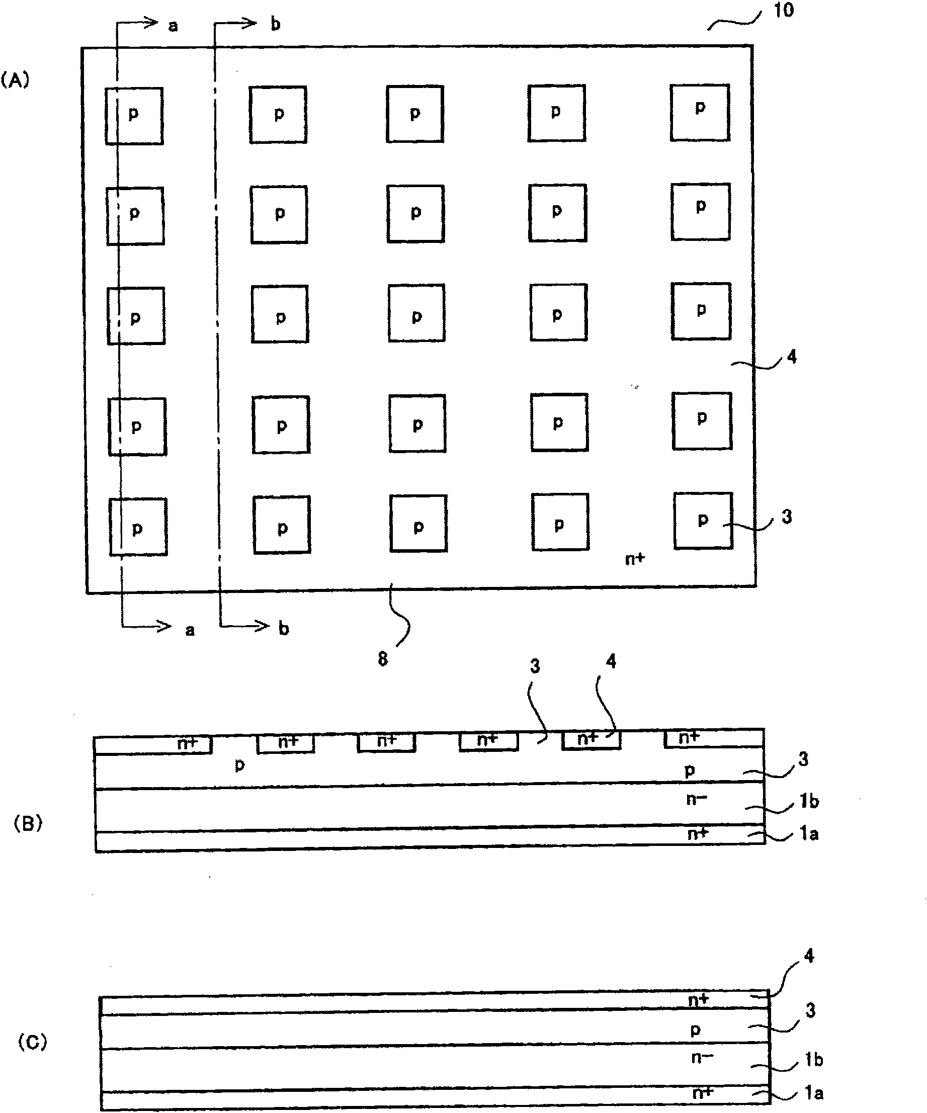
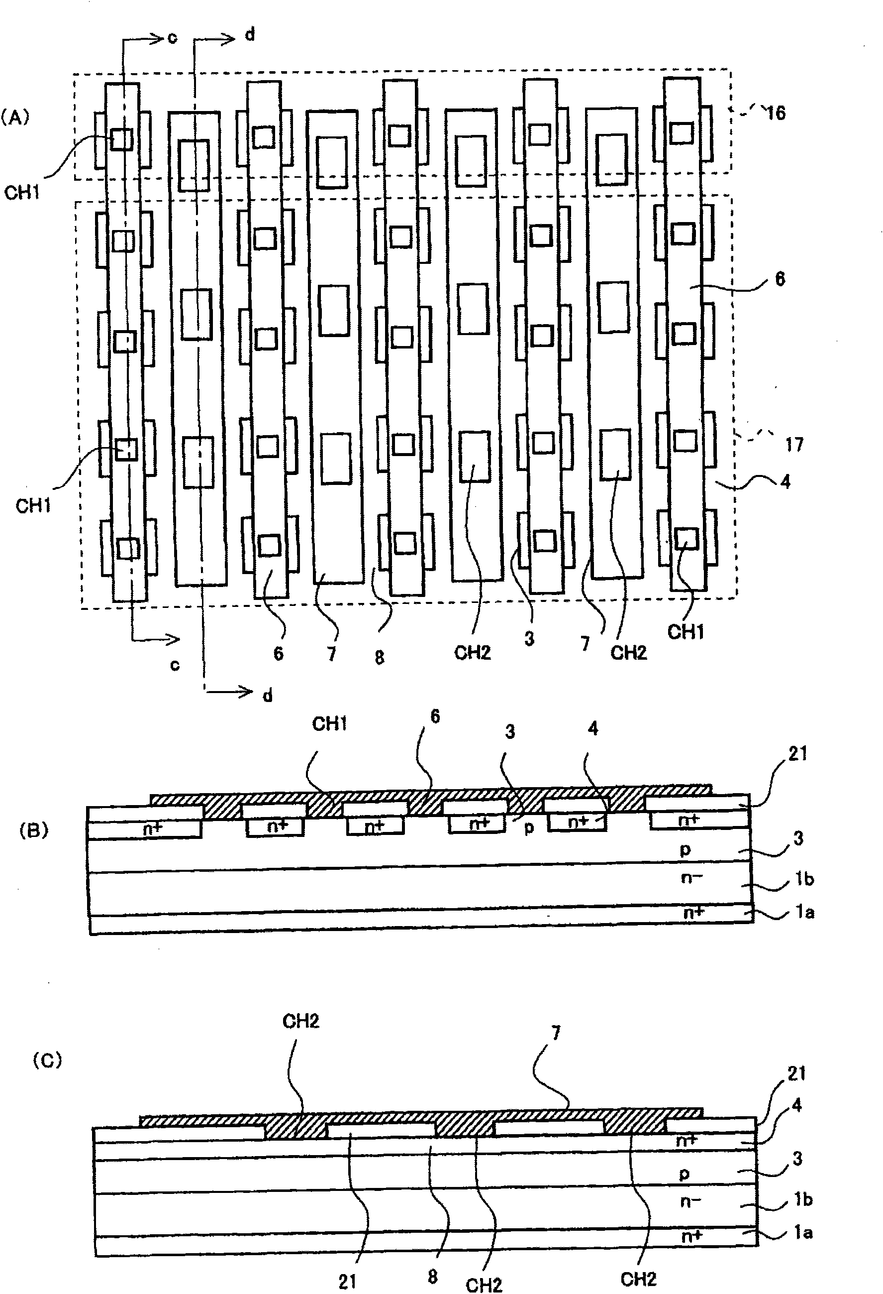
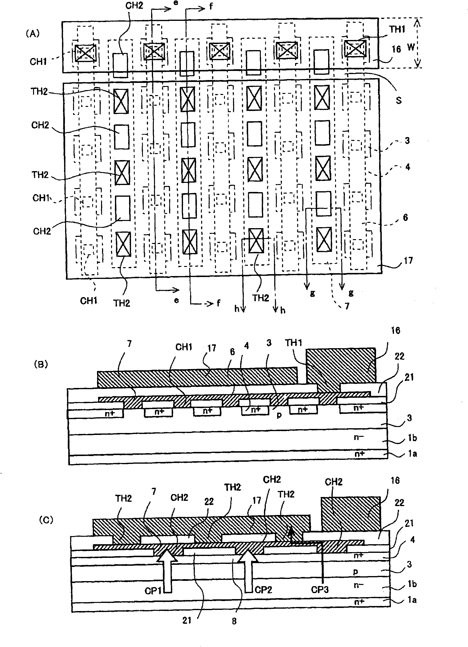
[0065] refer to Figure 1 to Figure 5 Embodiments of the present invention will be described in detail. In this embodiment, as the semiconductor device 10 , an npn-type bipolar transistor, which is a discrete element, will be described as an example.
[0066] figure 1 It is a figure showing the structure of the semiconductor device 10 which is this Example. figure 1 is a graph representing the action region, figure 1 (A) is a floor plan, figure 1 (B) is figure 1 (A) a-a line profile, figure 1 (C) is figure 1 (A) The b-b line profile.
[0067] The semiconductor device 10 is composed of the following components: a conductive semiconductor substrate, a base region, an emitter region, a first insulating film, a base contact hole, an emitter contact hole, a first base electrode, a first emitter electrode, a first Two insulating films, a base through hole, an emitter through hole, a second emitter electrode, a second base electrode, a conductive adhesive material, and...
PUM
 Abstract
Description
Claims
Application Information
 - Generate Ideas
- Intellectual Property
- Life Sciences
- Materials
- Tech Scout
- Unparalleled Data Quality
- Higher Quality Content
- 60% Fewer Hallucinations
Browse by: Latest US Patents, China's latest patents, Technical Efficacy Thesaurus, Application Domain, Technology Topic, Popular Technical Reports.
© 2025 PatSnap. All rights reserved.Legal|Privacy policy|Modern Slavery Act Transparency Statement|Sitemap|About US| Contact US: help@patsnap.com