


Quick Research
Generate reliable direction feasibility study reports for your R&D in just a few steps.

Technical Q&A
Discover and master advanced knowledge NOW. Basics, ideas, possibilities, all at once.

Find Solutions
As an expert in R&D theories, this can generate solutions to your technical problems instantly.

Evaluate Feasibility
Analyze your overall solution with one click, know your potential R&D risks in advance.

Monitor Landscape
Get weekly tech updates, stay abreast of the latest tech innovations and key insights.
Locking detector of phase-locked loop (PLL) and detection method thereof
A technology of detectors and phase-locked loops, which is applied to the detection of lock-in detectors and the field of lock-in detectors
- Summary
- Abstract
- Description
- Claims
- Application Information
AI Technical Summary
Problems solved by technology
Method used
Image

Examples
Embodiment 1
[0053] The invention discloses a phase-locked loop lock-in detector and its lock-in detection method. By introducing programmable technology in multiple places and rationally dividing the functional structure of the lock-in detector, the huge flexibility in the application of the lock-in detection circuit is finally realized. and portability.
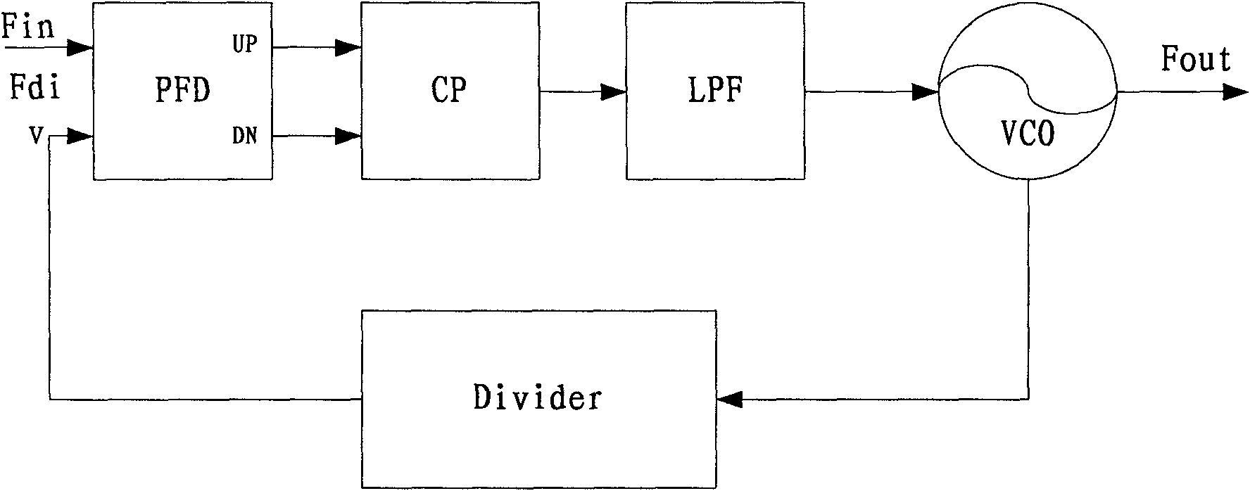
[0054] Such as figure 1 As shown, the phase-locked loop PLL includes a phase frequency detector PFD, a charge pump CP, a low-pass filter LPF, a voltage-controlled oscillator VCO, and a frequency divider Divider. The frequency and phase detector PFD generates the output control signal UP and the control signal DN by comparing the phase difference between the reference clock Fin and the feedback clock Fdiv generated by the frequency division of the VCO to control the switch of the upper / lower current source of the charge pump CP; The DN signal also maintains logic "1" for a set time when there is no phase difference between Fref and Fdiv...
Embodiment 2
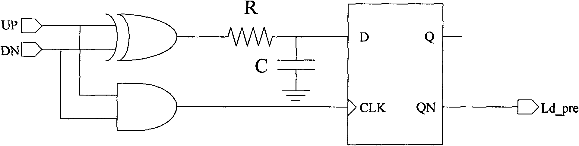
[0071] In this embodiment, the schematic diagram of the composition of the locking detector of the phase-locked loop is as follows figure 2 shown.
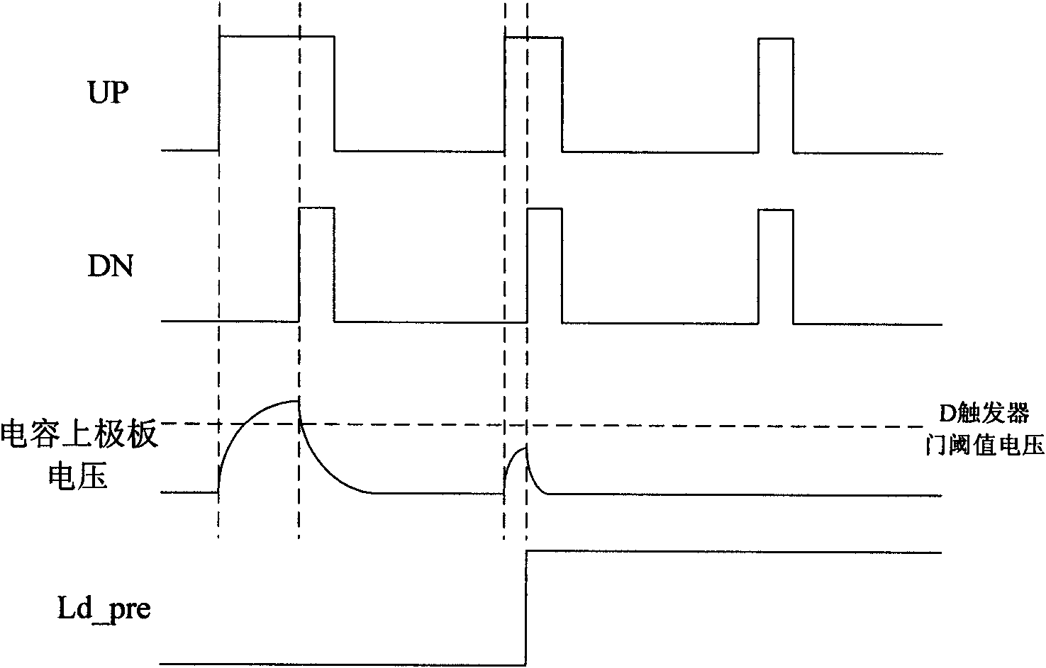
[0072] Since the time difference between the UP signal and the DN signal maintaining logic "1" indicates the phase difference between Fref and Fdiv, an exclusive OR gate circuit is used to collect the time when the UP signal and the DN signal are logic "1" alone. This time It is proportional to the phase difference between Fref and Fdiv. When one of the UP or DN signals is at high level and the other is at low level, the XOR gate outputs high level, thereby driving the charging resistor R behind it to charge the charging capacitor C. This charging process will be maintained until when the UP and DN signals are logic "1" at the same time, at this time the AND gate will generate a clock rising edge to drive the D flip-flop to sample the level on the capacitor to determine the difference between Fref and Fdiv Whether the phase dif...
PUM
 Abstract
Description
Claims
Application Information
 - R&D Engineer
- R&D Manager
- IP Professional
- Industry Leading Data Capabilities
- Powerful AI technology
- Patent DNA Extraction
Browse by: Latest US Patents, China's latest patents, Technical Efficacy Thesaurus, Application Domain, Technology Topic, Popular Technical Reports.
© 2024 PatSnap. All rights reserved.Legal|Privacy policy|Modern Slavery Act Transparency Statement|Sitemap|About US| Contact US: help@patsnap.com