Magnetron sputtering apparatus
A magnetron sputtering device and magnet technology, applied in sputtering coating, vacuum evaporation coating, coating, etc.
- Summary
- Abstract
- Description
- Claims
- Application Information
AI Technical Summary
Problems solved by technology
Method used
Image


Examples
no. 1 Embodiment approach
[0097] A first embodiment of the present invention will be described with reference to the drawings.
[0098] figure 1 It is a sectional view explaining the structure of the 1st Embodiment of the magnetic rotation sputtering apparatus of this invention.
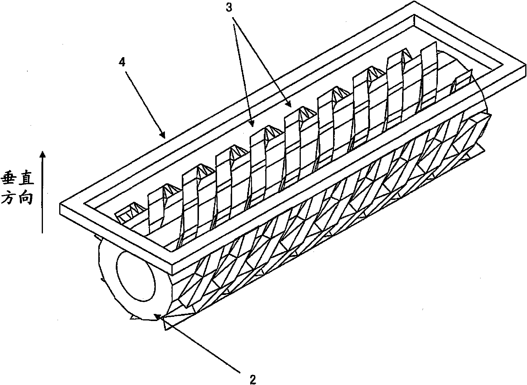
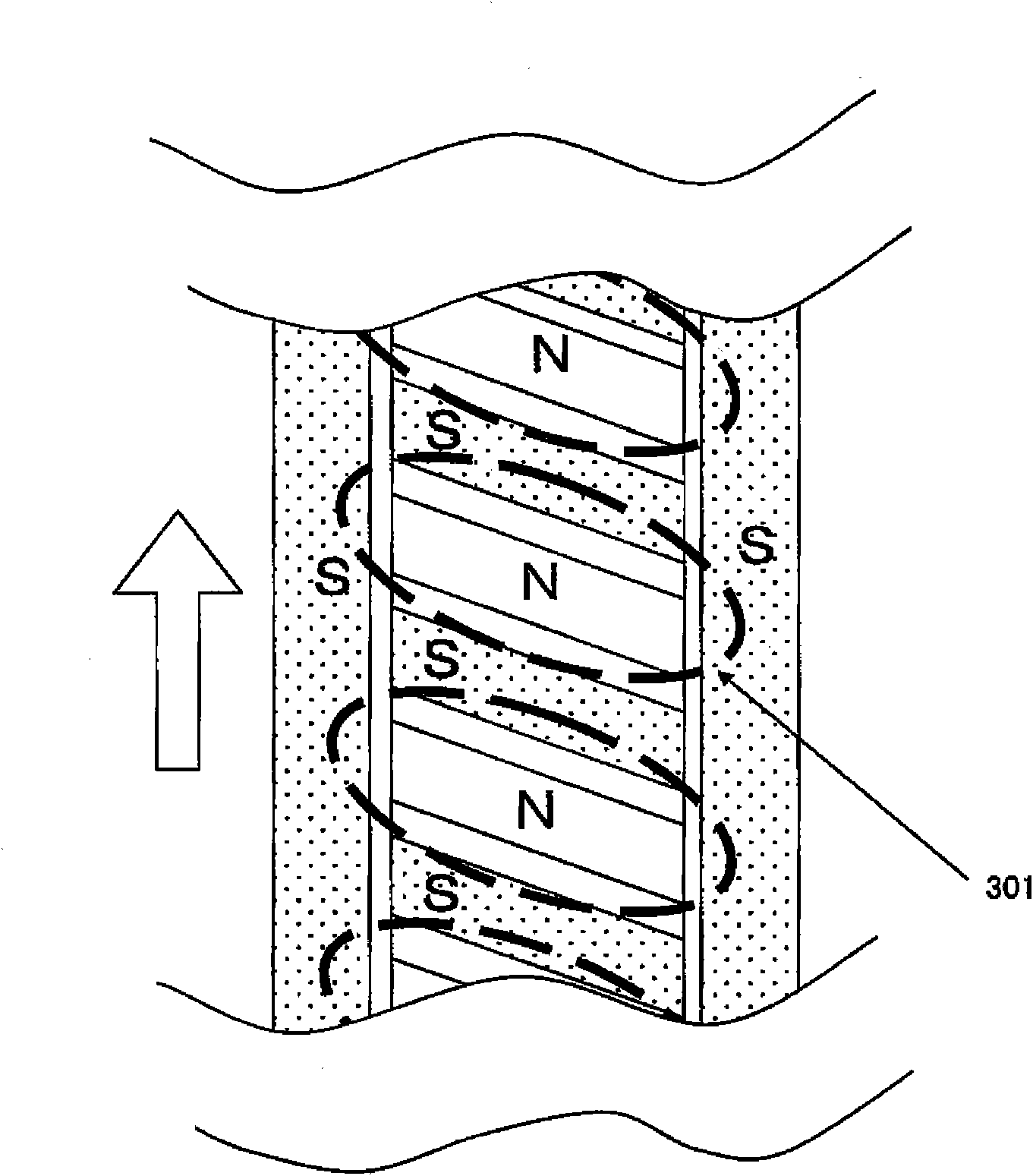
[0099] exist figure 1 Among them, 1 is a target, 2 is a cylindrical rotating shaft, 3 is a plurality of helical plate magnet groups arranged in a spiral shape on the surface of the rotating shaft 2, 4 is a fixed outer peripheral plate magnet arranged on the outer periphery, and 5 is a fixed outer peripheral plate magnet. The opposite side of the target of the magnet 4 is oppositely arranged on the outer peripheral permanent magnet on the fixed outer peripheral plate magnet 4, 6 is a packaging plate bonded to the target 1, and 15 is formed to cover the columnar rotating shaft 2 and the part other than the above-mentioned target side. The permanent magnet of the structure of the helical plate magnet group 3, 8 is the passag...
no. 2 Embodiment approach
[0120] Next, a second embodiment of the present invention will be described in detail with reference to the following drawings. Wherein, for convenience of description, parts overlapping with the above-mentioned embodiments are omitted. exist Figure 9 In the present embodiment shown, the slot width 20 and length of the slot 18 are set so that when the substrate to be processed is fixed and the helical plate magnet group is rotated at a certain frequency, no gap is blocked when the substrate to be processed is blocked. The area on the substrate that is less than 80% of the maximum film thickness formed per unit time. In this embodiment, the target material is pure aluminum. Below, combine Figure 10 for a more detailed explanation.
[0121] Figure 10 It is the film formation rate distribution in the direction perpendicular to the axis of the columnar rotation axis when the silicon substrate is installed at a position 30 mm away from the target surface. The above-mention...
no. 3 Embodiment approach
[0125] Next, a third embodiment of the present invention will be described in detail with reference to the following drawings. However, for the convenience of description, the description of the part overlapping with the above-mentioned embodiment is omitted. Rotary magnetron sputtering device of the present invention such as Figure 13 As shown, it is particularly suitable for use as a reciprocating film forming device.
[0126] exist Figure 13 Among them, 401 is a processing chamber, 402 is a gate valve, 403 is a substrate to be processed, and 404 is a rotating magnet plasma excitation part shown in the third embodiment. However, in the first embodiment, the axial length of the helical portion is 307 mm, but it is 270 mm in this example. The frequency of the plasma excitation power is 13.56 MHz. From the viewpoint of increasing the density of plasma and lowering the temperature of electrons, it is desirable to adopt a high frequency such as about 100 MHz, but the plasma...
PUM
 Abstract
Description
Claims
Application Information
 - R&D
- Intellectual Property
- Life Sciences
- Materials
- Tech Scout
- Unparalleled Data Quality
- Higher Quality Content
- 60% Fewer Hallucinations
Browse by: Latest US Patents, China's latest patents, Technical Efficacy Thesaurus, Application Domain, Technology Topic, Popular Technical Reports.
© 2025 PatSnap. All rights reserved.Legal|Privacy policy|Modern Slavery Act Transparency Statement|Sitemap|About US| Contact US: help@patsnap.com