Sample and hold circuit and digital-to-analog converter circuit
A technology of sampling and holding circuit and sampling voltage, which is applied in the direction of digital-to-analog converter, electrical analog memory, logic circuit connection/interface layout, etc., which can solve the problems of output error and achieve the effect of small output error
- Summary
- Abstract
- Description
- Claims
- Application Information
AI Technical Summary
Problems solved by technology
Method used
Image


Examples
Embodiment 1
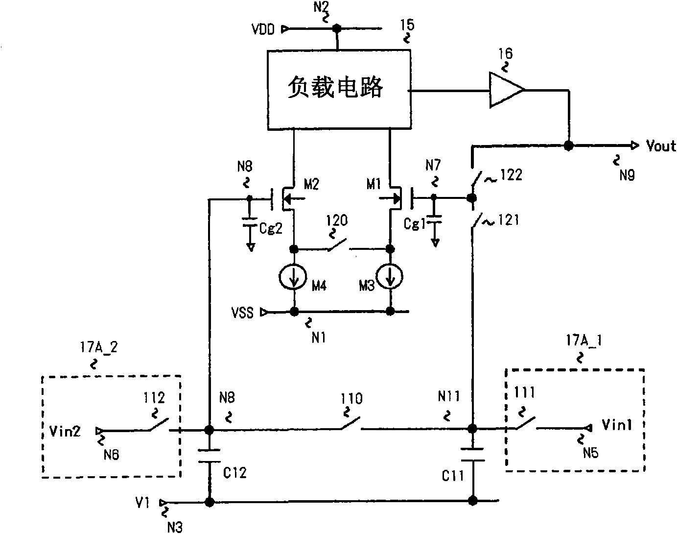
[0065] figure 1 It is a figure which shows the structure of one Example of this invention. It has n-channel MOS transistors M1 and M2, load circuit 15, amplifier stage 16, sampling voltage supply circuit 17, current sources M3 and M4, capacitors C11 and C12, and switches 110, 120, 121, 122. n channel. The MOS transistors M1 and M2, the load circuit 15, the differential stage constituted by the current sources M3 and M4, the amplifier stage 16, and the switches 120, 121, 122 constitute a differential circuit.
[0066] The drains of the n-channel MOS transistors M1 and M2 constituting the differential input stage are connected to the power supply node N2 of the power supply VDD through the load circuit 15, the sources are respectively connected to the power supply node N1 of the low-voltage power supply VSS through the current sources M3 and M4, and the gate poles are connected to nodes N7, N8. Capacitance Cg1 , Cg2 between nodes N7 , N8 and VSS represents gate parasitic cap...
Embodiment 2
[0098] Image 6 yes means Figure 5 The diagram of the configuration of the application circuit of , switches the non-inverting input / inverting input of the differential pair (M1, M2) at a predetermined cycle. exist Figure 5 In , the gate of the MOS transistor M1 is an inverting input, and the gate of the MOS transistor M2 is a non-inverting input, but in this embodiment, they are switched at a predetermined cycle.
[0099] refer to Image 6 , has: a switch 124, connected between the output node N9 and the gate (node N8) of the MOS transistor M2; a switch 123, connected between the gate of the MOS transistor M2 and one end (node N2) of the capacitor C12; switch 111 , connected between one end (node N11) of capacitor C11 and node N5; switch 117, connected between one end (node N12) of capacitor C12 and node N5; switch 118, connected between one end (node N11) and node N5 of capacitor C11 Between the nodes N6; the switch 112 is connected between one end of the cap...
Embodiment 3
[0111] Figure 8 It is a figure which shows the structure of the 3rd Example of this invention. In the present embodiment, the sampling voltage supply circuit 17C controls ON / OFF of the switches 113 and 114 based on the bit data of the digital signal serially input during the sampling period. There is a switch 114 between the node N4 and the node N11, and a switch 113 between the node N11 and the node N3. The current values of the current sources M3 and M4 are set to be equal to each other, and the capacitance values of the capacitors C11 and C12 are set to be equal to each other. The sampling voltage supply circuit 17C may be connected to the node N8.
[0112] Figure 9 It is explained from the point of view of switch control Figure 8 diagram of the action. The period T0-T2 is a data sampling period, the switch 121 is turned on, and the switches 120 and 122 are turned off.
[0113] In the period T0-T2 (reset period), the switches 110 and 113 are turned on and the s...
PUM
 Abstract
Description
Claims
Application Information
 - R&D
- Intellectual Property
- Life Sciences
- Materials
- Tech Scout
- Unparalleled Data Quality
- Higher Quality Content
- 60% Fewer Hallucinations
Browse by: Latest US Patents, China's latest patents, Technical Efficacy Thesaurus, Application Domain, Technology Topic, Popular Technical Reports.
© 2025 PatSnap. All rights reserved.Legal|Privacy policy|Modern Slavery Act Transparency Statement|Sitemap|About US| Contact US: help@patsnap.com