Liquid crystal display panel
A liquid crystal display panel and display area technology, applied in static indicators, nonlinear optics, instruments, etc., can solve the problem that the liquid crystal display panel fails to fully discharge electrostatic charges, and achieve the effect of preventing damage and fully releasing
- Summary
- Abstract
- Description
- Claims
- Application Information
AI Technical Summary
Problems solved by technology
Method used
Image
Examples
Embodiment Construction
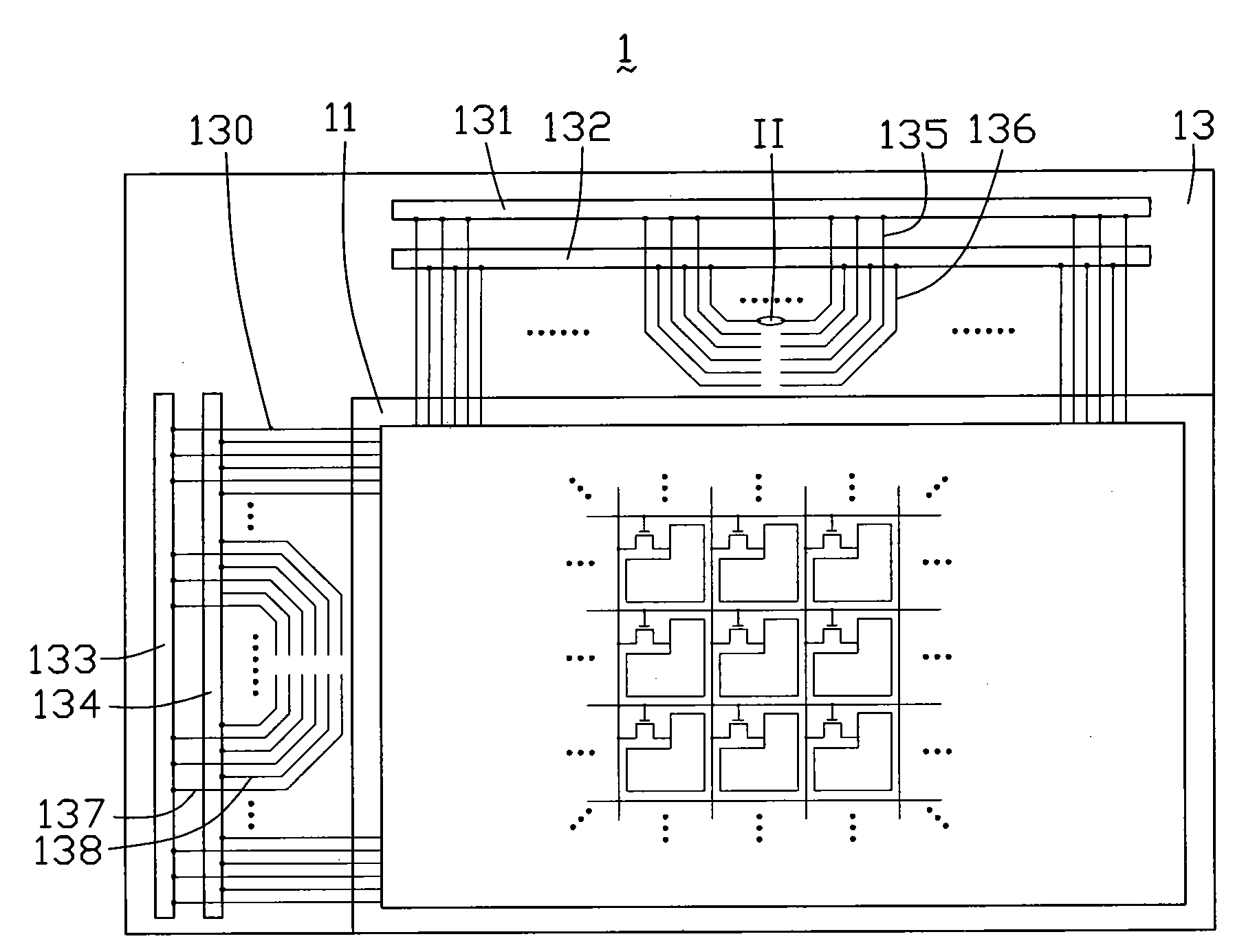
[0014] see figure 1 and figure 2 , figure 1 It is a structural schematic diagram of the first embodiment of the liquid crystal display panel of the present invention, figure 2 yes figure 1 The enlarged schematic diagram of region II is shown. The LCD panel 1 includes a display area 11 and a non-display area 13 adjacent to the display area 11 .
[0015] The display area 11 includes a plurality of scan driving lines (not marked), a plurality of data driving lines (not marked) and a plurality of thin film transistors (not marked). The plurality of scanning driving lines are arranged parallel to each other, and the data driving lines and the scanning driving lines are respectively arranged perpendicular to each other, wherein the minimum area enclosed by the intersection of the scanning driving lines and the data driving lines defines a pixel area (not shown). The thin film transistors are respectively located in each pixel area. The scan driving line transmits a scan volt...
PUM
 Abstract
Description
Claims
Application Information
 - Generate Ideas
- Intellectual Property
- Life Sciences
- Materials
- Tech Scout
- Unparalleled Data Quality
- Higher Quality Content
- 60% Fewer Hallucinations
Browse by: Latest US Patents, China's latest patents, Technical Efficacy Thesaurus, Application Domain, Technology Topic, Popular Technical Reports.
© 2025 PatSnap. All rights reserved.Legal|Privacy policy|Modern Slavery Act Transparency Statement|Sitemap|About US| Contact US: help@patsnap.com


