Control logical circuit and successive approximation analog-to-digital converter

A technology for controlling logic circuits and circuits, applied in analog/digital conversion, code conversion, instruments, etc., can solve problems such as operation optimization without consideration of correlation, smaller setup and hold time margins, increased power consumption, etc., to avoid Timing check step, reduction of gate count, effects of saving area and power consumption

Inactive Publication Date: 2010-01-06
WUXI ZGMICRO ELECTRONICS CO LTD
View PDF0 Cites 9 Cited by
  • Summary
  • Abstract
  • Description
  • Claims
  • Application Information

AI Technical Summary

Problems solved by technology

[0013] However, for asynchronous circuits, due to the existence of multiple clock domains, the delay of each node signal relative to each clock domain may need to be considered, so the check of the setup and hold time of each node signal becomes complicated accordingly, different The more clock domains, the related paths to be checked will increase in proportion; at the same time, because the timing correlation is complex, there will be greater uncertain time between different clock domains, which leads to a smaller margin for setup and hold times. Make asynchronous circuits slower than synchronous circuits
[0014] For synchronous circuits, since the known synchronous circuits are all realized through RTL (RegisterTransfer Level, register transfer level) synthesis, there are redundant standard units, and no consideration is given to performing operations based on the correlation between adjacent cycles. Optimization, resulting in the operation unit not being reused, wasting area and increasing additional power consumption

Method used


Image

  • Control logical circuit and successive approximation analog-to-digital converter
  • Control logical circuit and successive approximation analog-to-digital converter
  • Control logical circuit and successive approximation analog-to-digital converter

Examples


Embodiment Construction

[0053] In order to make the above objectives, features and advantages of the present invention more obvious and understandable, the present invention will be further described in detail below with reference to the accompanying drawings and specific embodiments.

[0054] The core idea of ​​the present invention is that the successive approximation mode and synchronous control logic are still adopted in the principle realization, but the simplified control logic and the simplified circuit are realized in the specific circuit structure to reduce the complexity of the overall circuit.

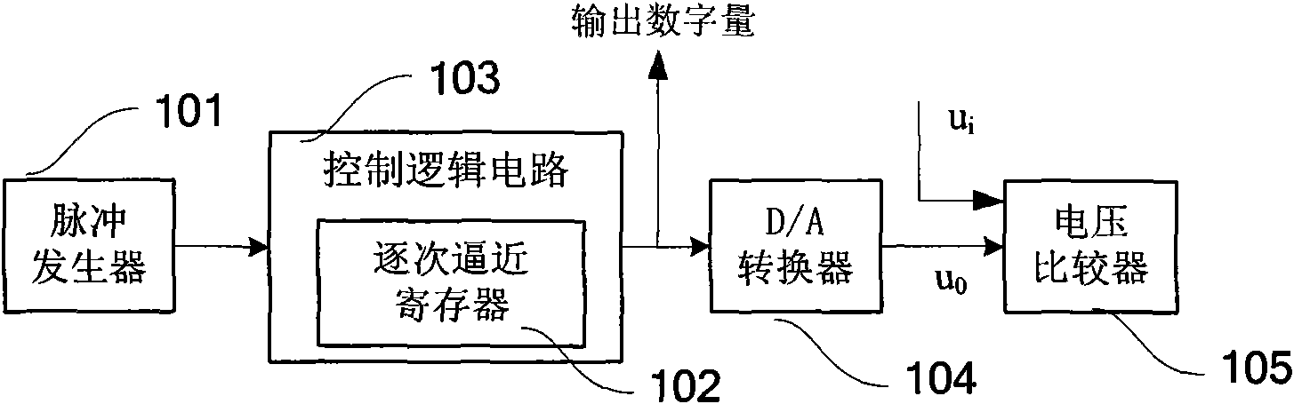
[0055] Reference figure 1 , Shows a structural block diagram of an embodiment of a successive approximation analog-to-digital converter of the present invention. It can specifically include:

[0056] The pulse generator 101 is used to generate a clock pulse signal and a start signal to start conversion;

[0057] The successive approximation register 102 is used to store the converted binary value of each d...


PUM


Abstract

The invention provides a control logical circuit placed in a successive approximation analog-to-digital converter and comprising a starting circuit and N basic cell circuits which are connected sequentially. The starting circuit is used for starting analog-to-digital conversion according to a conversion request signal and a clock signal, and the basic cell circuits are used for completing the binary numeric conversion of corresponding digit bits in a corresponding clock cycle, receiving the feedback signal of a comparator, and adjusting the values of the corresponding digit bits; wherein each basic cell circuit also comprises a trigger Q8 used for storing and outputting corresponding bit values of corresponding successive approximation codes in different clock cycles. The N basic cell circuits comprise N circuits which are connected sequentially from a cell (N-1) circuit to a cell (0) circuit, wherein the cell (0) also comprises an ACK output port, and an initial assignment circuit is connected with a cell (N-2) circuit, etc., a cell (1) circuit and the cell (0) circuit and is used for generating initial assignment signals aiming at each basic cell circuit.

Description

Technical field [0001] The present invention relates to the technical field of mutual conversion between analog signals and digital signals, in particular to a control logic circuit of an analog-to-digital conversion device and a successive approximation analog-to-digital converter. Background technique [0002] Analog-to-digital conversion is a technology that converts an analog input signal into an N-bit binary digital output signal. The use of digital signal processing can facilitate the realization of various advanced adaptive algorithms and complete functions that cannot be achieved by analog circuits. Therefore, more and more analog signal processing is being replaced by digital technology. Correspondingly, the application of analog-to-digital conversion as a bridge between analog and digital systems is becoming more and more extensive. [0003] Generally, analog-to-digital conversion includes four processes: sampling, holding, quantization and programming: [0004] A. Sampli...

Claims


Application Information

Patent Timeline
Patent Type & Authority Applications(China)
IPC IPC(8): H03K19/003H03M1/38
Inventor 赵纲
Owner WUXI ZGMICRO ELECTRONICS CO LTD
Why Eureka
Try Eureka