
Electromagnetic wave mask

An electromagnetic wave, mask technology, used in electrical components, printed circuit components, magnetic field/electric field shielding, etc.

Inactive Publication Date: 2009-11-04
WISTRON CORP
View PDF0 Cites 4 Cited by
  • Summary
  • Abstract
  • Description
  • Claims
  • Application Information

AI Technical Summary

Problems solved by technology

Therefore, the known electromagnetic interference shield still has room for improvement

Method used


Image

  • Electromagnetic wave mask
  • Electromagnetic wave mask
  • Electromagnetic wave mask

Examples


Embodiment Construction

[0022] The invention relates to an electromagnetic wave mask. In order to make the present invention easier to understand, the preferred embodiments of the technology of the present invention will be described in detail below with illustrations. However, the illustrations and detailed descriptions are not intended to limit the technology and various changes and modifications disclosed in the present invention.

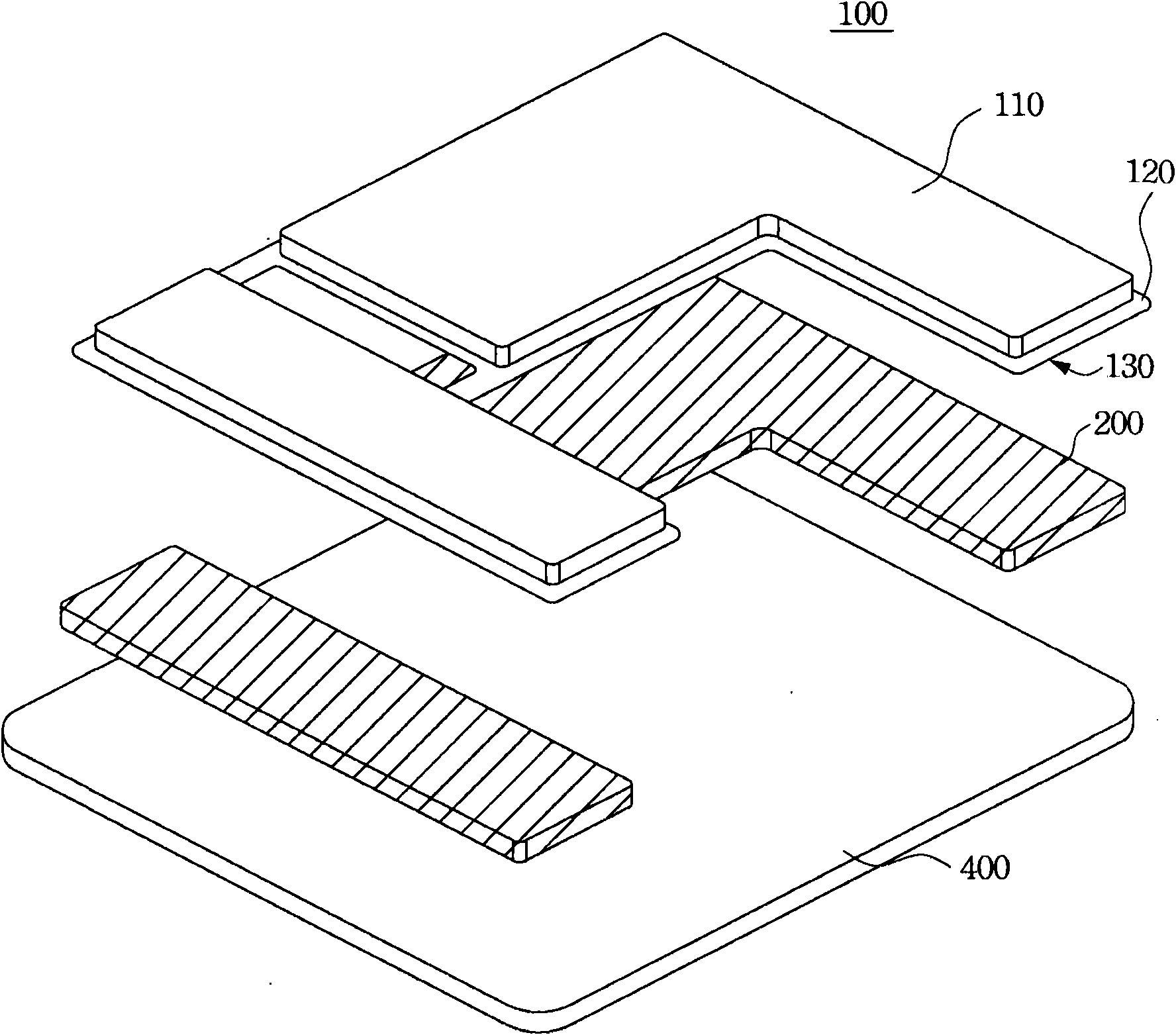
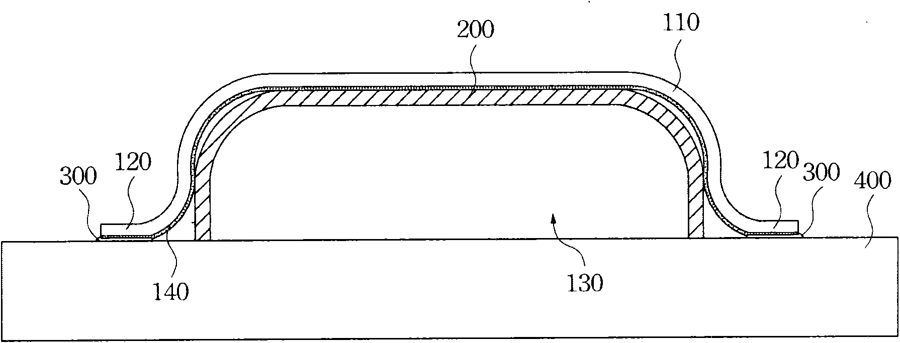
[0023] With reference figure 2 , which is a schematic diagram of components of the electromagnetic wave mask of the present invention. As shown in the figure, the electromagnetic wave mask 100 proposed by the present invention is covered on a printed circuit board 400 to shield the electronic components on the printed circuit board 400 from electromagnetic interference (Electromagnetic Interference, EMI). The electromagnetic wave mask 100 of the present invention is at least composed of a shielding cover 110 , an insulating layer 200 , and a conductive glue 300 (not...


PUM


Abstract

The invention discloses an electromagnetic wave mask which at least comprises a shielding cover, an insulating layer and a conductive adhesive, wherein the protrudent cover edge of the shielding cover is hermetically pasted on a printed circuit board with the conductive adhesive; and the insulating layer is arranged between the shielding cover and the printed circuit board to enable the shielding cover not to be contacted with the printed circuit board to provide electromagnetic interference (EMI) for shielding the printed circuit board. The design of the electromagnetic wave mask can decrease the height combined with the circuit board by passing the protrudent cover edge of the shielding cover on the printed circuit board with the conductive adhesive.

Description

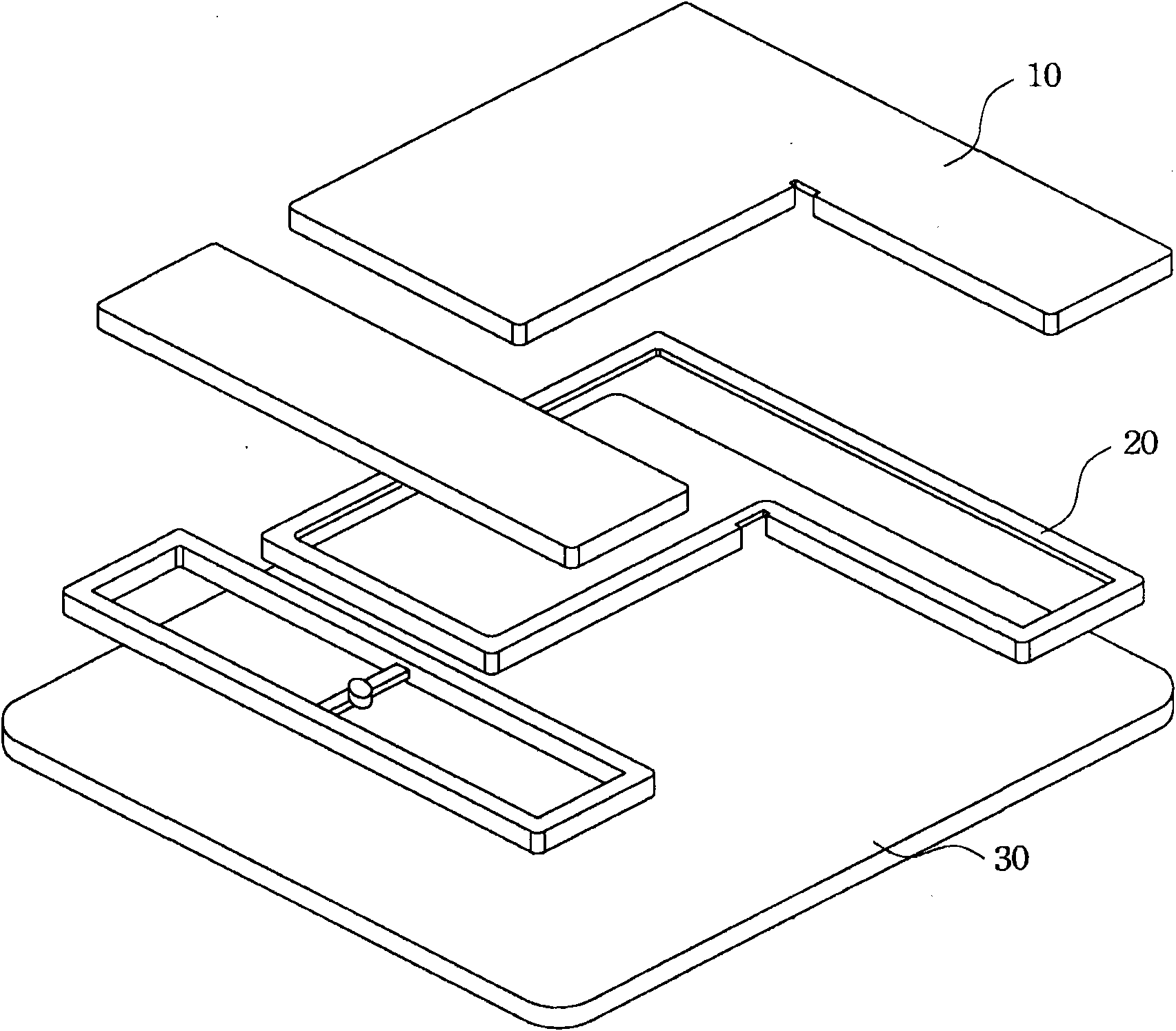
technical field [0001] The present invention relates to an electromagnetic wave mask, in particular to an electromagnetic wave mask arranged on a printed circuit board for shielding electromagnetic interference (EMI). Background technique [0002] In the current electromagnetic interference (EMI) prevention and control countermeasures in electronic products, generally speaking, in order to reduce the interference of external electromagnetic fields or static electricity on the operation of important electronic components on the circuit board of electronic products, it is usually necessary to place Covering with an electromagnetic interference shielding cover. And the known electromagnetic interference shielding cover mostly uses tinplate, the metal cover of nickel-nickel metal stamping and forming, and its setting method, such as figure 1 As shown, the electromagnetic interference shielding cover 10 is soldered to the reserved ground on the printed circuit board 30 through t...

Claims


Application Information

Patent Timeline
Patent Type & Authority Applications(China)
IPC IPC(8): H05K9/00H05K1/02
Inventor 曾天仲
Owner WISTRON CORP
Learn More