Method for producing transparent substrate double-sided conductive film of touch control circuit

A technology of transparent substrates and touch circuits, which is applied to circuits, semiconductor/solid-state device manufacturing, electrical components, etc., can solve the problems of consuming process man-hours and material costs, and achieve the effects of reducing costs, reducing man-hours, and simplifying the layout process

Inactive Publication Date: 2009-10-21
TPK LENS SOLUTIONS INC
View PDF0 Cites 26 Cited by
  • Summary
  • Abstract
  • Description
  • Claims
  • Application Information

AI Technical Summary

Problems solved by technology

[0004] However, in the above-mentioned traditional touch circuit manufacturing method, the steps of attaching and removing the photoresist layer and the protective layer must be repeated for many times, and the development and etching processes must be repeated for many times, which consumes man-hours and material costs. question

Method used


Image

  • Method for producing transparent substrate double-sided conductive film of touch control circuit
  • Method for producing transparent substrate double-sided conductive film of touch control circuit
  • Method for producing transparent substrate double-sided conductive film of touch control circuit

Examples


Embodiment Construction

[0035] The steps of the manufacturing method of the double-sided conductive film of the transparent substrate of the touch circuit of the present invention and the effects that can be produced are described in detail as follows with a preferred embodiment in conjunction with the accompanying drawings:

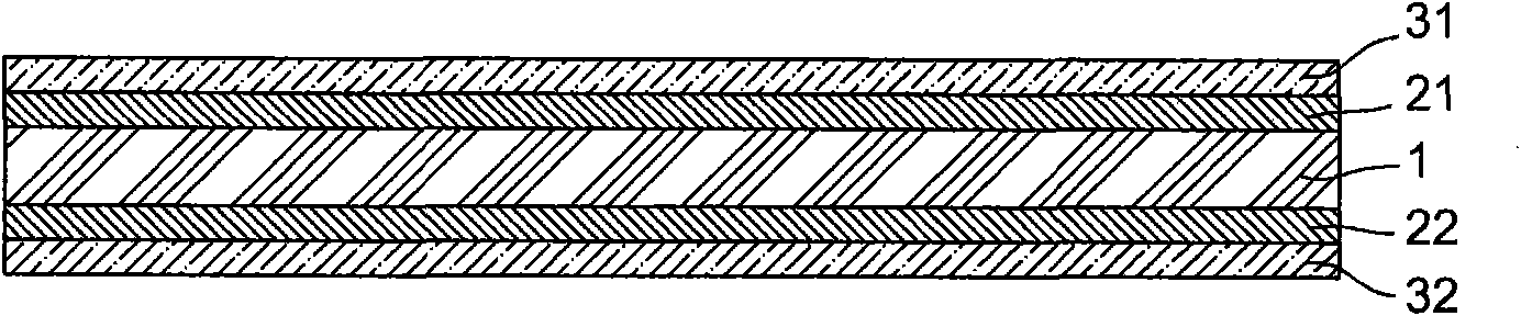
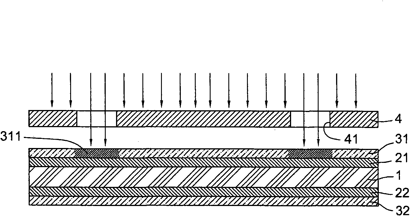
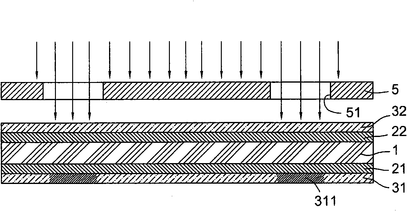
[0036] see figure 1 As shown, it is a cross-sectional view of the configuration state of the embodiment of the present invention, and cooperates with Figure 2 to Figure 6 The method for preparing the double-sided conductive film of the transparent substrate of the touch circuit of the present invention includes the following steps:

[0037] (1) A transparent substrate 1 is placed in the sputtering equipment, and a first conductive substrate layer is formed on the first surface of the transparent substrate 1 by vacuum sputtering; in this implementation, the transparent substrate 1 The first surface is located on the top surface of the transparent substrate 1, and the first con...


PUM


Abstract

The invention discloses a method for producing a transparent substrate double-sided conductive film of a touch control circuit, comprising the following steps: attaching a first photoresistive layer with photosensitive colour-changing agent on a fist conductive substrate layer of a first surface of a transparent substrate and attaching a second photoresistive layer on a second conductive substrate of a second surface of the transparent substrate; exposing the first photoresistive layer to enable the first photoresistive layer to receive the exposure area to form a circuit pattern with identification colors; exposing the second photoresistive layer by utilizing the circuit pattern of the first exposing as the contraposition reference of the exposure of the second photoresistive layer; developing and etching the double sides of the transparent substrate to enable the first conductive substrate layer to form a first conductive film of a touch control circuit, and forming a second conductive film of the touch control circuit on the second conductive substrate layer. The invention simplifies the laying procedures of the touch control circuit, thereby having the advantages of reduction of labor hour and reduction of cost.

Description

technical field [0001] The present invention relates to a method for manufacturing a touch circuit, in particular to a method for manufacturing a conductive film forming a touch circuit on both sides of a transparent substrate by means of sputtering, exposure, development, etching and the like. Background technique [0002] Now common touch panels are usually resistive and capacitive touch panels. Among them, the resistive touch panel can press the surface of the panel with fingers, pens or other media to generate touch signals, but compared with the resistive touch panel, the capacitive touch panel only needs to touch the surface of the panel with fingers. A slight touch can generate a touch signal, which has better sensitivity in use; therefore, there are more advanced mobile phones, global positioning systems (GPS), personal digital assistants (Personal Digital Assistant, PDA), palm-sized Touch panels of electronic products such as Palm-Sized PCs and Information Applianc...

Claims


Application Information

Patent Timeline
Patent Type & Authority Applications(China)
IPC IPC(8): G06F3/044H01L21/00H01L21/3213H01L21/84
Inventor 周祎平
Owner TPK LENS SOLUTIONS INC
Why Eureka
Try Eureka