
High chamber temperature process and chamber design for photo-resist stripping and post-metal etch passivation

A technology of process gas and chamber body, applied in the direction of discharge tubes, electrical components, circuits, etc., can solve the problems of increasing the overall complexity of chamber design and manufacturing costs.

Active Publication Date: 2009-09-02
LAM RES CORP
View PDF1 Cites 27 Cited by
  • Summary
  • Abstract
  • Description
  • Claims
  • Application Information

AI Technical Summary

Problems solved by technology

Those requirements often lead to the selection of more expensive insulation materials and / or complex cooling mechanisms, increasing the overall complexity of the chamber design and manufacturing costs

Method used


Image

  • High chamber temperature process and chamber design for photo-resist stripping and post-metal etch passivation
  • High chamber temperature process and chamber design for photo-resist stripping and post-metal etch passivation
  • High chamber temperature process and chamber design for photo-resist stripping and post-metal etch passivation

Examples


Embodiment Construction

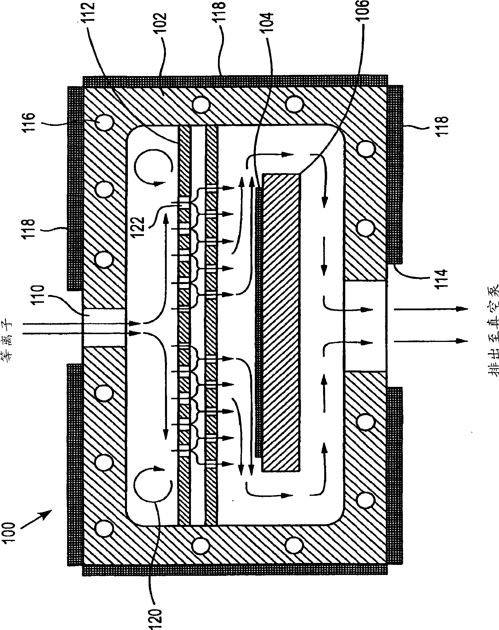
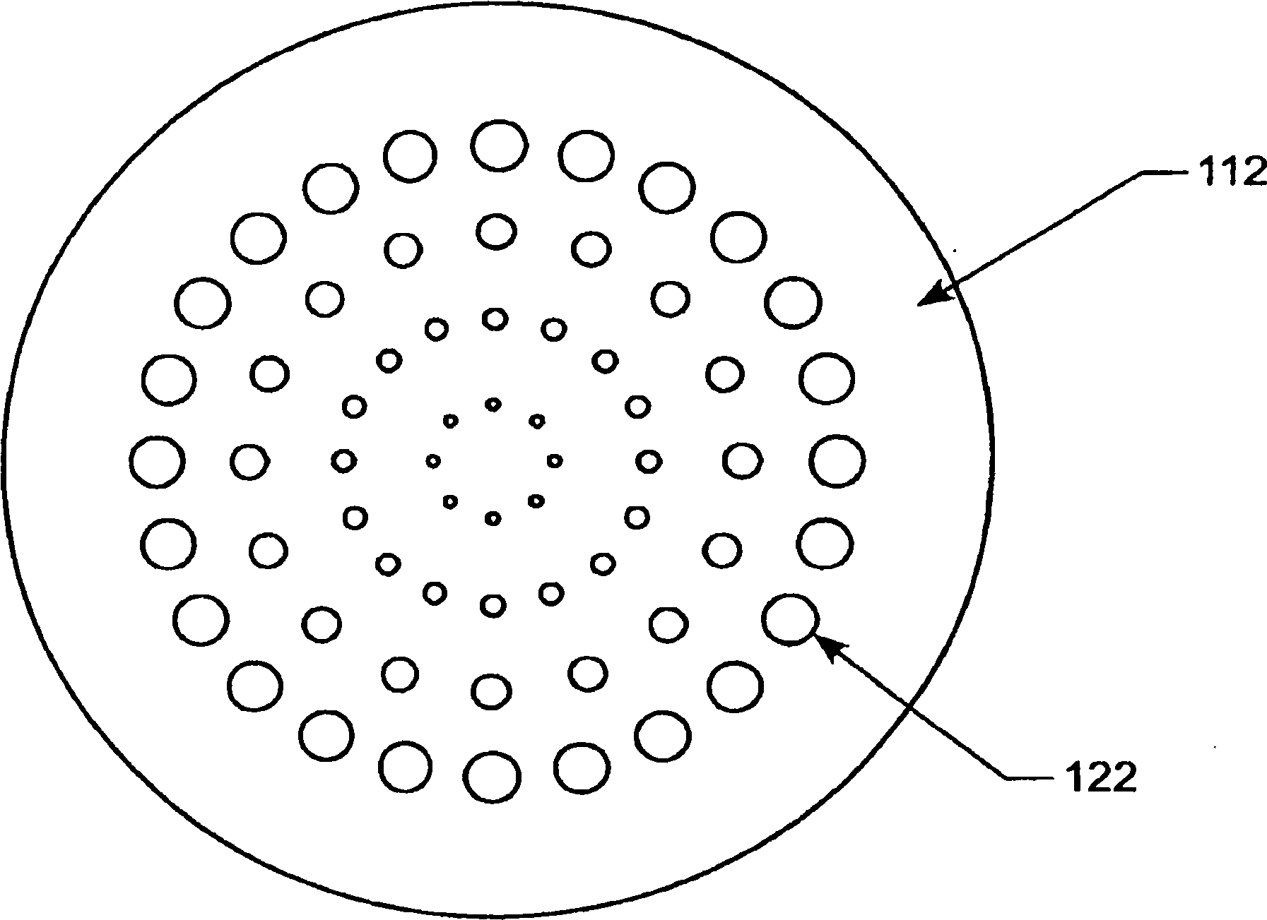
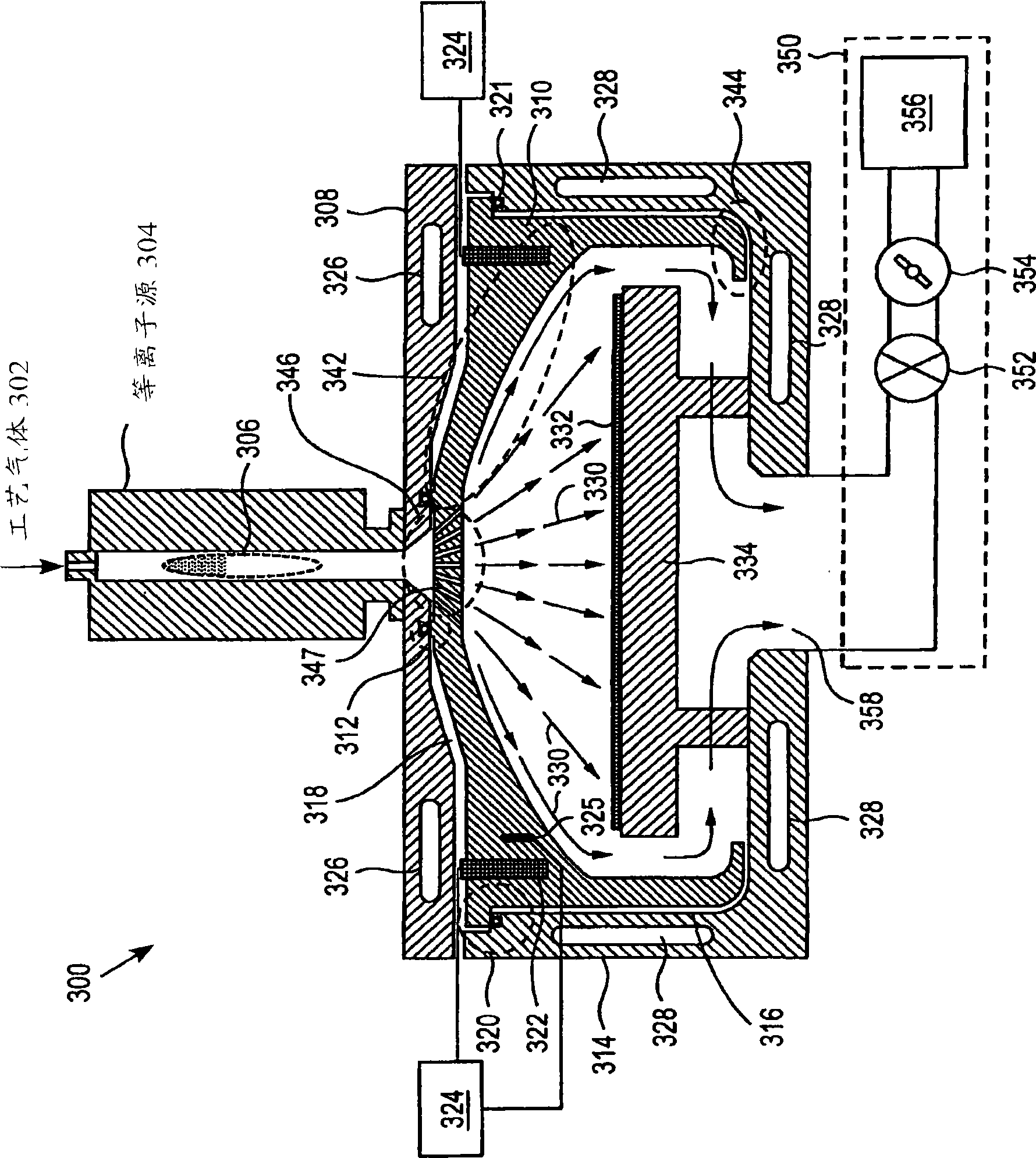
[0016] A strip chamber is described for increasing the stripping rate of photoresist on a substrate disposed within the chamber. Certain embodiments may include, inter alia, a gas distribution assembly having a very small surface area exposed to the gas, and including a plurality of gas channels formed therein, wherein the gas fans out as the gas passes through the channels. The stripping chamber may also include an inner chamber body that forms a dome-shaped cavity to further fan the gas and thereby provide a uniform distribution of gas flow over the surface of the substrate. The "dome-shaped" cavity preferably has a width or diameter that decreases away from the substrate, ie the cavity may be conical, hemispherical, concave or other shape.

[0017] In stripping or ashing processes using a gas, the gas can have a high flow rate and high pressure, creating a high gas velocity at the opening of the downstream stripping chamber. In some applications, this velocity can be as hi...


PUM


Abstract

A vacuum chamber for passivation and / or stripping a photoresist layer formed on a semiconductor substrate. The chamber includes an internal chamber body that forms a cavity to surround the substrate and has a plurality of gas passages extending therethrough to the cavity and one or more heaters to heat the internal chamber body. The internal chamber body is slidably mounted on an external chamber body that surrounds a side of the internal chamber with a gap therebetween. The device also includes: an exhaust unit operative to pump the gas from the cavity; a chamber top mounted on the internal chamber body to cover a top surface of the internal chamber body with a gap therebetween and having an opening in fluid communication with the gas passages; and a plasma source operative to energize the gas into a plasma state and coupled to the opening for fluid communication with the cavity.

Description

Background technique [0001] Integrated circuits are formed from wafers or substrates on which patterned microelectronic layers are formed. In the process of fabricating these integrated circuits, a patterned photoresist layer is typically used as a masking layer in order to form those patterned layers from a previously deposited capping layer. After forming a patterned layer on a substrate, the corresponding photoresist layer can be removed from the substrate in a strip chamber or asher before proceeding to the next process. [0002] Since photoresist stripping is frequently used in semiconductor fabrication shops, strippers or stripping chambers are designed to have very short process times (ie, high throughput) to reduce overall substrate fabrication costs. Thus, the performance of a downstream plasma stripping chamber is often determined by its stripping rate, which is defined as the photoresist stripping rate per unit time. The strip rate determines how long the substrat...

Claims


Application Information

Patent Timeline
IPC IPC(8): H01L21/76
CPCH01J37/00H01J37/3244H01J37/16H01J37/32834H01J37/32449H01L21/02H01L21/3065
Inventor 英岩艾伯特·王罗伯特·谢彼
Owner LAM RES CORP
Learn More