
Method for producing high multilayered blind hole multilayer board by double head pressing insertion pin

A multi-layer board and high multi-layer technology is applied in the direction of multi-layer circuit manufacturing and electrical connection formation of printed components. It can solve problems such as poor hole wall quality, difficulty in chip removal, and decreased electroplating efficiency, so as to solve protection problems and manufacture The effect of process optimization and reduction of scrap rate

Active Publication Date: 2009-08-05
SHENNAN CIRCUITS
View PDF0 Cites 11 Cited by
  • Summary
  • Abstract
  • Description
  • Claims
  • Application Information

AI Technical Summary

Problems solved by technology

[0002] When making PCB high-layer and high-thickness backplanes, due to the number of layers and high thickness of the board, the alignment between layers during lamination is a very big challenge
At the same time, when the through hole is made after pressing, due to the large thickness-to-aperture ratio, the difficulty of drilling and electroplating increases: the increase in hole depth makes it difficult to remove chips during drilling, and the quality of the hole wall is poor; at the same time, the electroplating solution cannot The smooth circulation in the hole leads to a decrease in the plating efficiency; while the blind hole is difficult to process, the residual liquid in the blind hole cannot be cleaned, resulting in oxidation on the board surface and inside the hole
Summarizing the above reasons, when the thickness-to-aperture ratio of the PCB high-layer backplane exceeds a certain limit value, the process of making through holes is complicated and difficult to realize.

Method used


Image

  • Method for producing high multilayered blind hole multilayer board by double head pressing insertion pin
  • Method for producing high multilayered blind hole multilayer board by double head pressing insertion pin
  • Method for producing high multilayered blind hole multilayer board by double head pressing insertion pin

Examples


Embodiment Construction

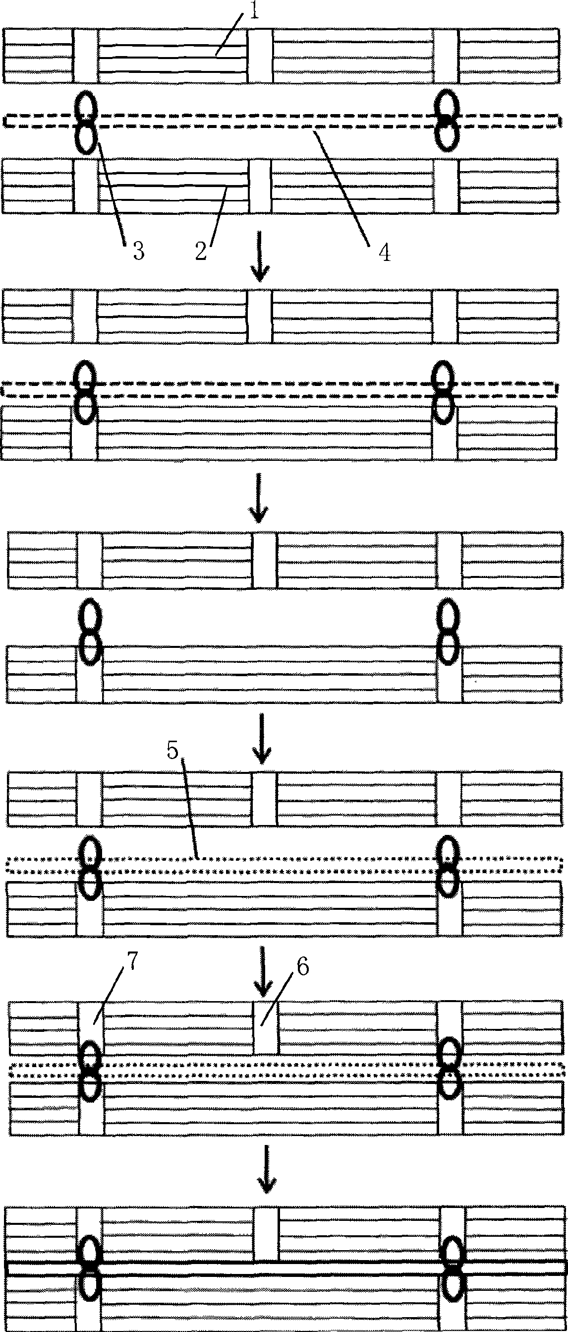
[0014] like image 3 As shown in the figure, the method of making high-level multi-layer blind-hole multilayer boards by double-headed crimping pins is to divide a backplane into several sub-boards. After the sub-boards are fabricated through drilling, electroplating and surface treatment, Then, the upper and lower sub-boards are crimped to the upper and lower sub-boards through the double-ended pressing pins 3, and then lamination and pressing are carried out to finally form the mother board. The other holes without pressing pins become blind holes. After pressing, the board can be used directly without wet treatment.

[0015] Using double-ended press pins, first put the tool board 4 (such as image 3 shown) drilling, only drill through hole 7 when drilling, do not drill blind hole 6, insert the double-ended press pin 3 into the tool 4 board, and press the double-ended press insert on the tool board 4 through the cooperation of the positioning holes Press one end of pin 3 int...


PUM


Abstract

The invention discloses a method for adopting a double head pressure contact pin to produce a multi-layer plate for a multi-layer dead hole. A backboard is divided into a plurality of sub-plates. When the sub-plates is produced by hole drilling, galvanization, surface treatment and other procedures, the double head pressure contact pin is used for pressing and being connected with an upper sub-plate and a lower sub-plate for purpose of lamination and press so as to finally form a motherboard. The holes at corresponding positions of the upper sub-plate and the lower sub-plate can together form an integral through hole though the double head pressure contact pin. The other holes in which no contact pins are inserted are dead holes. The pressed plates can be used directly without wet treatment. The invention can improve the contraposition, drilling and galvanization of the high multi-layer backboard, solves the problem on the protection of mechanical dead holes, optimizes the backboard production procedures, improves the productivity and reduces the product scrap rate.

Description

technical field [0001] The invention relates to a method for manufacturing a printed circuit, in particular to a method for manufacturing a high-multi-layer blind-hole multilayer board by means of double-ended crimping pins. Background technique [0002] When making high-layer and high-thickness PCB backplanes, due to the large number of layers and high thickness of the board, the alignment between layers during lamination is a very big challenge. At the same time, when making through-holes after pressing, due to the large thickness-to-diameter ratio of the plate, the difficulty of drilling and electroplating increases: the increase of hole depth makes it difficult to remove chips during drilling, and the quality of the hole wall is poor; The smooth flow in the hole leads to a decrease in the electroplating efficiency; however, it is difficult to process the blind hole, and the residual liquid medicine in the blind hole cannot be cleaned, resulting in oxidation of the board ...

Claims


Application Information

Patent Timeline
IPC IPC(8): H05K3/42H05K3/46
Inventor 彭勤卫史庚才孔令文
Owner SHENNAN CIRCUITS
Learn More