Equipment for etching uniwafer of silicon wafer back face

A backside, silicon wafer technology, used in electrical components, semiconductor/solid-state device manufacturing, circuits, etc., can solve the problems of dielectric film etching and affect the quality of the dielectric film on the back of the product, and achieve the effect of reducing over-etching and ensuring quality.

Inactive Publication Date: 2009-06-24
SHANGHAI HUA HONG NEC ELECTRONICS
View PDF0 Cites 2 Cited by
  • Summary
  • Abstract
  • Description
  • Claims
  • Application Information

AI Technical Summary

Problems solved by technology

However, such a process treatment method will inevitably cause the dielectric film that needs to be retained in the lower layer to be etched, thereby affecting the quality of the dielectric film on the back of the product.

Method used


Image

  • Equipment for etching uniwafer of silicon wafer back face
  • Equipment for etching uniwafer of silicon wafer back face
  • Equipment for etching uniwafer of silicon wafer back face

Examples


Embodiment Construction

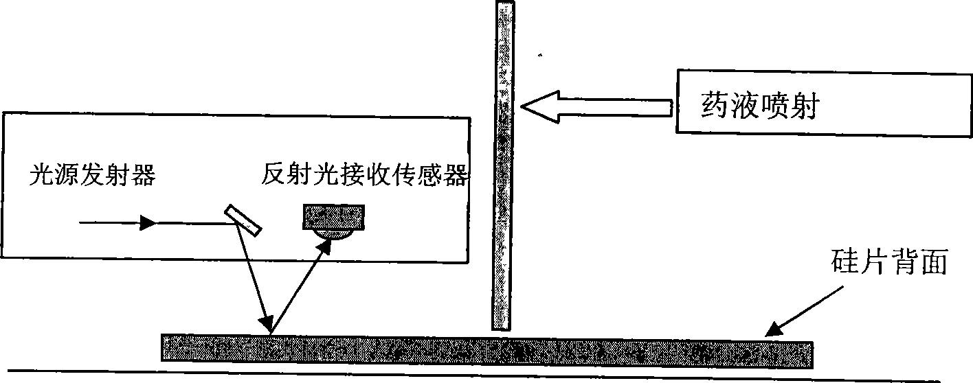
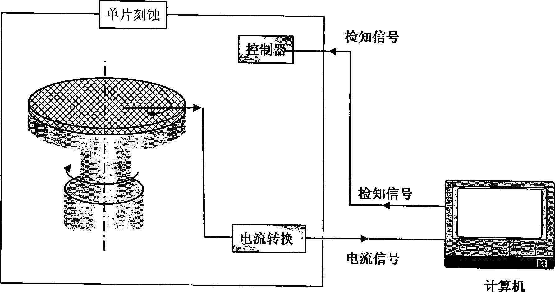
[0013] Such as figure 1 , 2 As shown, the silicon wafer back monolithic etching equipment of the present invention includes a controller, and also includes an endpoint detection device (EPD), which includes a light source emitter, a reflected light receiving sensor and a signal processing system, and the light source emits The device emits light to the back of the silicon wafer, and the reflected light receiving sensor is used to receive the reflected light emitted by different dielectric films on the back of the silicon wafer for the emitted light (see figure 1 ), and convert the information of the reflected light into a current signal and transmit it to the signal processing system, the signal processing system determines the end point detection result according to the reflected light information, and transmits the detection signal of the end point detection result to the controller (see figure 2 ), the controller controls the etching process of the chemical solution to st...


PUM


Abstract

The invention discloses a silicon wafer backside monolithic etching equipment, which comprises a controller and an endpoint detector; the endpoint detector comprises a light source transmitter, a reflected light receiving sensor and a signal processing system; the light source transmitter transmits light to the backside of the silicon wafer; the reflected light receiving sensor is used to receive the reflected light emitted from different medium films on the backside of the silicon wafer, and the reflected light aims at the emission light; then the reflected light receiving sensor transfers the information of the reflected light to the signal processing system; the signal processing system determines the endpoint detection result based on the reflected light information and transfers the endpoint detection result to the controller to control the etching process of medical liquid to stop at the dividing positions of different medium films. The silicon wafer backside monolithic etching equipment enables the medium films which need to be etched on the backside of the silicon wafer to be completely etched; at the same time, the equipment reduces the over-etching of the medical liquid on the medium film of the next layer and ensures the quality of the medium films kept on the backside of the product.

Description

technical field [0001] The invention relates to silicon wafer etching equipment, in particular to a silicon wafer back monolithic etching equipment. Background technique [0002] The silicon wafer back etching process currently used in the semiconductor manufacturing process mainly ensures that the dielectric film to be etched on the back of the silicon wafer is completely etched by increasing a certain amount of over-etching. However, such a process treatment method will inevitably cause the dielectric film that needs to be kept in the lower layer to be etched, thereby affecting the quality of the dielectric film on the back of the product. Contents of the invention [0003] The technical problem to be solved by the present invention is to provide a single-chip etching equipment on the back of a silicon wafer, which can completely etch the dielectric film to be etched on the back of the silicon wafer, and at the same time reduce the over-etching of the lower dielectric fi...

Claims


Application Information

Patent Timeline
Patent Type & Authority Applications(China)
IPC IPC(8): H01L21/00H01L21/306H01L21/311
Inventor 潘嘉王明琪刘须电
Owner SHANGHAI HUA HONG NEC ELECTRONICS
Why Eureka
Try Eureka