
General-purpose test board and its use method

A test board, general-purpose technology, used in electronic circuit testing, measuring electricity, measuring devices, etc.

Inactive Publication Date: 2009-06-24
SEMICON MFG INT (SHANGHAI) CORP
View PDF0 Cites 18 Cited by
  • Summary
  • Abstract
  • Description
  • Claims
  • Application Information

AI Technical Summary

Problems solved by technology

[0004] The purpose of the present invention is to provide a general-purpose test board and its use method, to solve the problem of needing to purchase a dedicated test board when testing packaged chips with different pin distributions

Method used


Image

  • General-purpose test board and its use method
  • General-purpose test board and its use method
  • General-purpose test board and its use method

Examples


Embodiment Construction

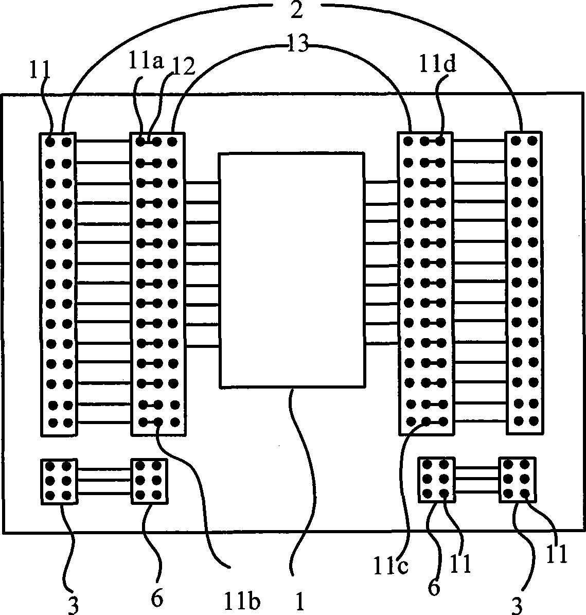
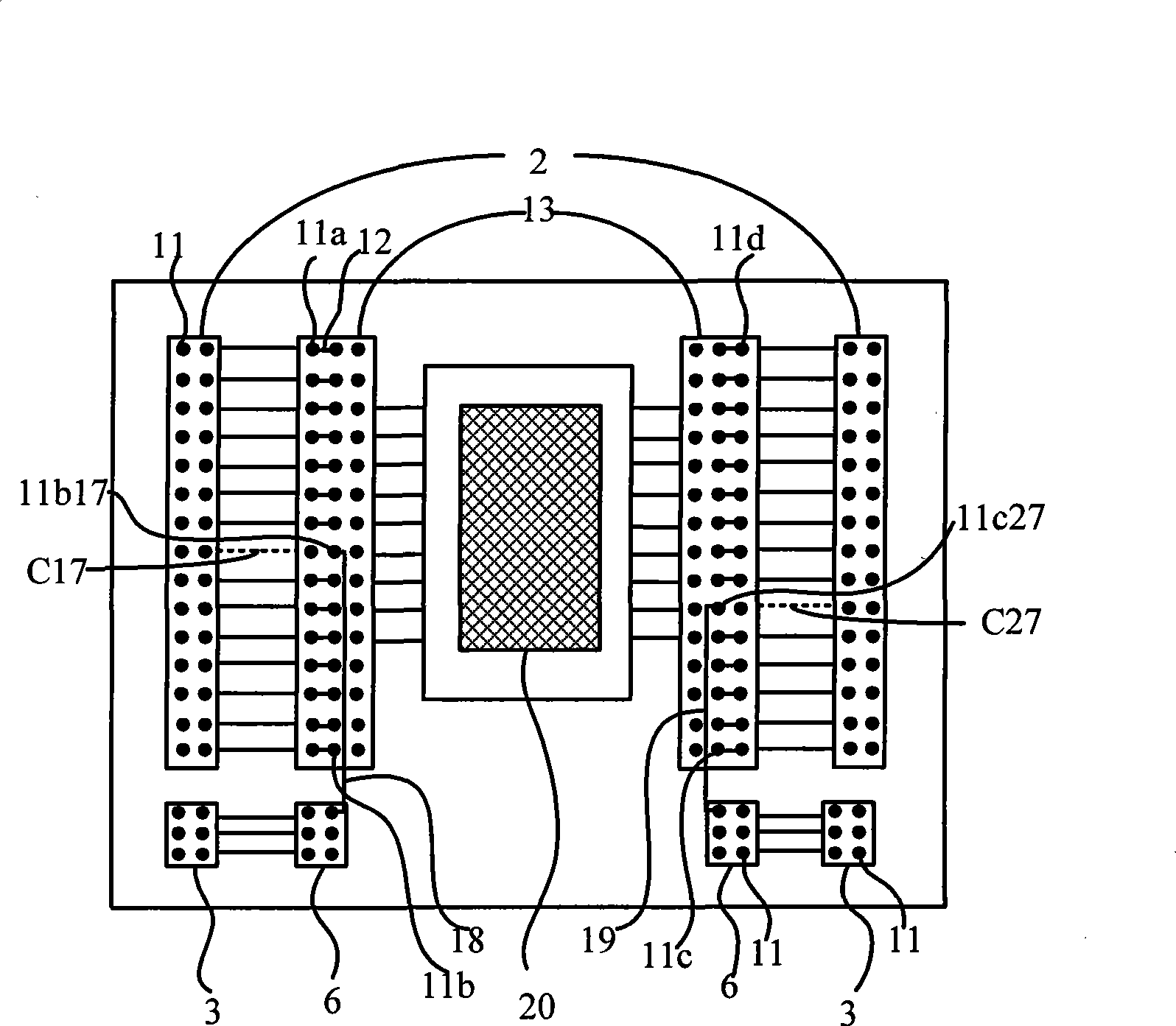
[0013] At present, DIP packaging is a commonly used packaging type in chip packaging. Take a general-purpose test board for testing DIP-packaged chips to be tested as an example. see figure 2 , this universal test board includes two connectors 2 with two columns of pins 11, two power connectors 3 with two columns of pins 11, chip sockets 1 with several pin slots and two with A buffer connector 13 with several rows of pins 11 and two power buffer connectors 6 with two rows of pins 11 . The buffer connector 13 is connected to the connector 2 and the chip socket 1 , and the power buffer connector 6 is connected to the power connector 3 . The pins of the power buffer connector 6 are connected to the pins of the power connector 3 .

[0014] The buffer connector 13 has three columns of pins and a group of connectors 12 (Jumper), wherein one column of pins 11a is connected to the connector 2, that is, one-to-one correspondingly connected with a column of pins of the connector 2; t...


PUM


Abstract

The invention relates to a universal type test board and a testing method thereof. The universal type test board can be used for testing encapsulating chips with base pins distributed differently, comprises a plurality of connectors with two columns of contact pins, a plurality of power connectors with two columns of contact pins and a chip socket, and further comprises a plurality of buffering connectors and a plurality of power buffering connectors. The buffering connectors are connected with the chip socket and the connectors; and the power buffering connectors are connected with the power connectors. When the chips are tested on the test board, the configuration of a power channel or a signal channel is conducted to the connecting channels of the contact pins on the buffering connectors through testing the distribution of the base pins of the chips. By adopting the method, the test board can test the various encapsulating chips with the base pins distributed differently, so that a special test board is not required when the chips with the base pins to be distributed are tested, thus effectively solving the testing economic cost of the chips.

Description

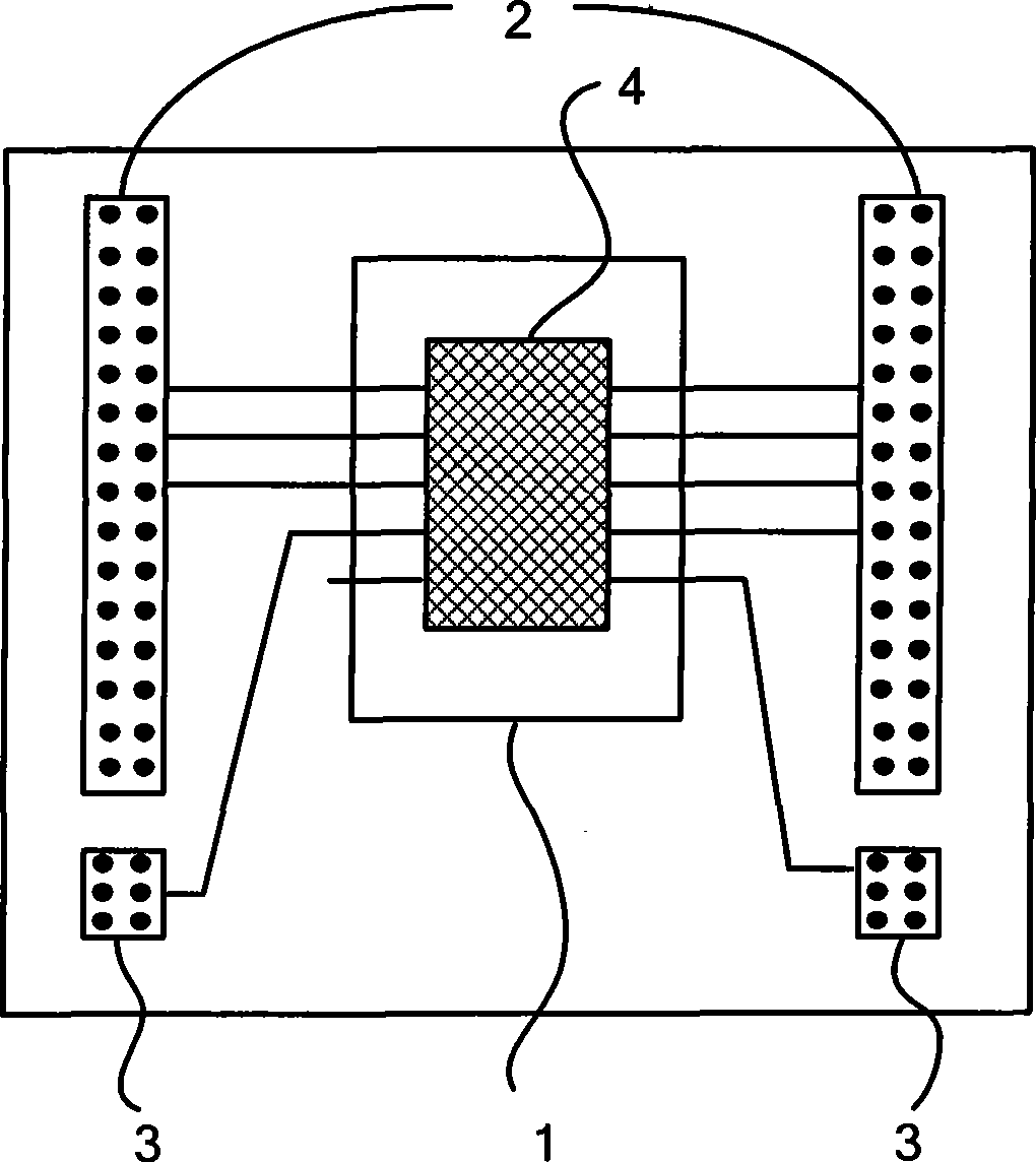
technical field [0001] The invention relates to the field of design and manufacture of chip testing devices, in particular to a universal testing board and a method for using the same. Background technique [0002] At present, packaging is required after the production of chips is completed, such as dual in-line packaging (DIP), quad flat packaging (QFP) or other types of packaging. Different chip package types have different pinouts and pin counts. These packaged chips are subject to functional verification and testing. When performing this operation, these packaged chips need to be placed on a specific test board for testing. Conventional test boards such as figure 1 As shown, it includes two connectors 2 (connectors), two power connectors 3 and chip socket 1. This type of test board targets dual in-line packaged chips. When testing, the chip 4 to be tested is placed on the chip socket 1 with several pin slots on the test board, and the two connectors are connected to...

Claims


Application Information

Patent Timeline
IPC IPC(8): G01R31/28G01R1/073G01R1/02
Inventor 何莲群刘云海
Owner SEMICON MFG INT (SHANGHAI) CORP
Learn More