Method for producing a monocrystalline or polycrystalline semiconductor material

A polycrystalline semiconductor, semiconductor technology, applied in the direction of polycrystalline material growth, crystal growth, single crystal growth, etc., can solve problems such as complex structure, achieve the effect of effective control, improved process parameter definition, and rapid melting

Inactive Publication Date: 2009-06-24
SCHOTT AG
View PDF15 Cites 5 Cited by
  • Summary
  • Abstract
  • Description
  • Claims
  • Application Information

AI Technical Summary

Problems solved by technology

However, the construction is more complex

Method used


Image

  • Method for producing a monocrystalline or polycrystalline semiconductor material
  • Method for producing a monocrystalline or polycrystalline semiconductor material
  • Method for producing a monocrystalline or polycrystalline semiconductor material

Examples


Embodiment Construction

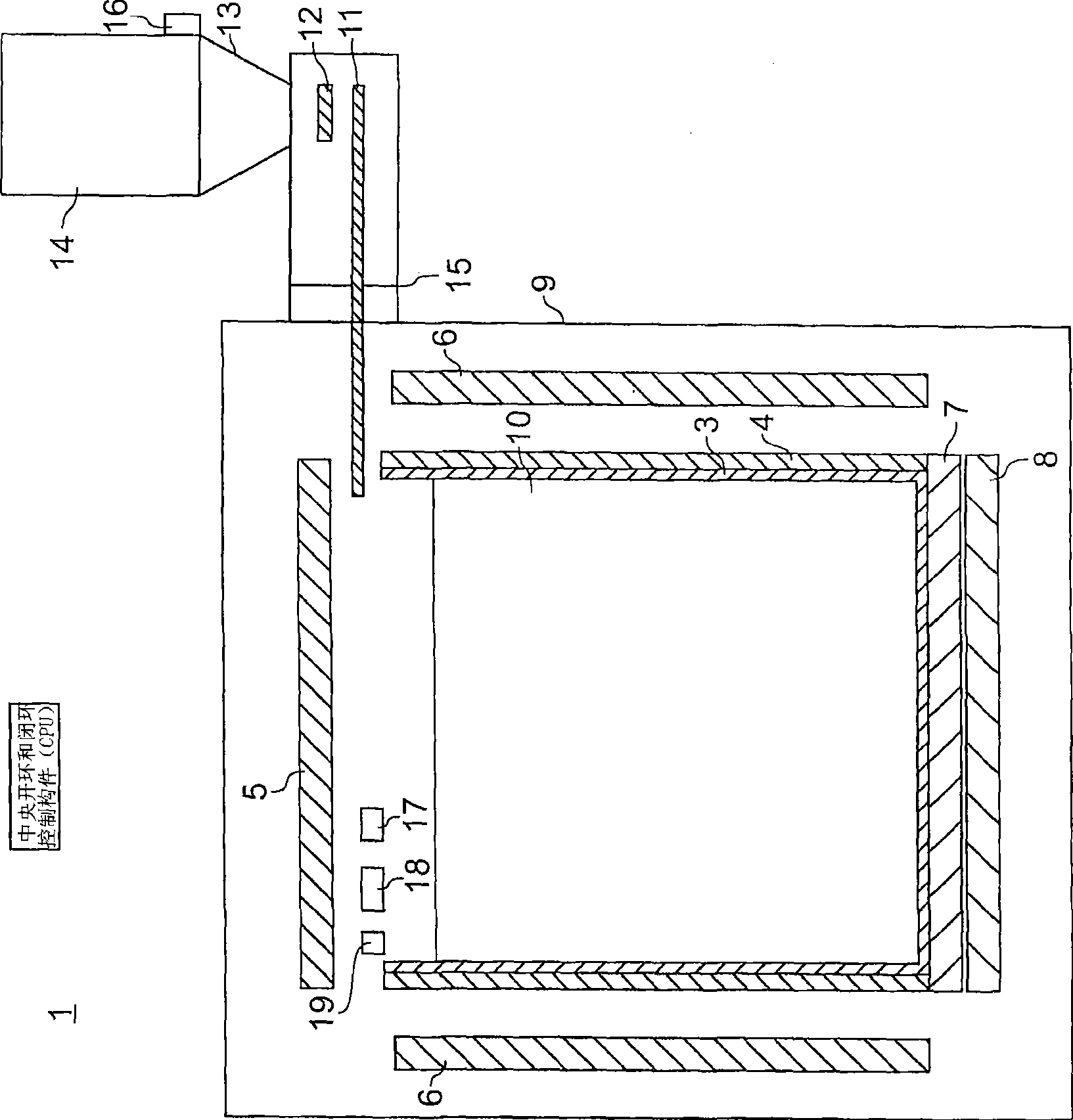
[0040] according to figure 1 , the crystallization system (whose whole is indicated by reference numeral 1) comprises a quartz crucible 3 completely and in close proximity contained in an upwardly open box-like support system 4, in order to provide a crystallization system already at the melting temperature of silicon The lower softened quartz crucible 3 provides sufficient mechanical support. The quartz crucible 3 reaches up to the upper edge of the support system 4, thus excluding direct contact of the silicon melt with graphite or other contaminating materials. Quartz crucible 3 is commercially available quartz crucible, and it has for example 550 * 550mm 2 、720×720mm 2 or 880×880mm 2 of the bottom area, and has an inner coating as the crucible SiO 2 between the silicon and the separator layer. The upper heater 5 is provided above the crucible, and its bottom area is greater than or equal to the bottom area of ​​the crucible. A jacketed heater 6 surrounding the crucib...


PUM


Abstract

The invention relates to a method for producing a monocrystalline or polycrystalline semiconductor material by way of directional solidification, wherein lumpy semiconductor raw material is introduced into a melting crucible and melted therein and directionally solidified, in particular using the vertical gradient freeze method. In order to prevent contamination and damage, the semiconductor raw material is melted from the upper end of the melting crucible. The molten material trickles downward, so that semiconductor raw material which has not yet melted gradually slumps in the melting crucible. In this case, the additional semiconductor raw material is replenished to the melting crucible from above onto a zone of semiconductor raw material which has not yet melted or is not completely melted, in order at least partly to compensate for a volumetric shrinkage of the semiconductor raw material and to increase the filling level of the crucible. In order to reduce the melting-on time and to influence the thermal conditions in the system as little as possible, the semiconductor raw material to be replenished is heated by the purposeful introduction of heat to a temperature below the melting temperature of the semiconductor raw material and introduced into the container in the heated state.

Description

[0001] This application claims the German patent application No. 10 2007 061 704.8 "Method for Producing a Monocrystalline or Polycrystalline Material" filed on December 19, 2007 and the application on May 8, 2008 German patent application No. 10 2008 022 882.6 "Method for Crystallization of a Semiconductor Material, in particular of Silicon" (Method for Crystallization of a Semiconductor Material, inparticular of Silicon), the entire content of which is incorporated by reference incorporated into this article. technical field [0002] The present invention relates to methods and apparatus for the manufacture of single or polycrystalline materials via directional solidification, in particular using a method known as the vertical gradient freezing method (hereinafter referred to as the VGF method), and in particular to the manufacture of Methods and apparatus for polysilicon. Background technique [0003] In general, solar cells for photovoltaics can be made of monocrystalli...

Claims


Application Information

Patent Timeline
Patent Type & Authority Applications(China)
IPC IPC(8): C30B11/00
CPCC30B28/06C30B11/04C30B29/06
Inventor 乌韦·萨赫尔马蒂亚斯·米勒英戈·施维利希弗兰克-托马斯·伦特斯弗兰克·比勒斯费尔德弗兰克-托马斯·伦特斯
Owner SCHOTT AG
Why Eureka
Try Eureka