Semiconductor image sensing device

A technology for imaging components and semiconductors, which is applied to semiconductor devices, electrical components, and electric solid-state devices, etc., can solve the problems of complex peripheral circuit composition, reduced detection accuracy, and difficulty in reducing the size of pixels, and achieves the effect of simple circuit composition.

Inactive Publication Date: 2009-05-27
KENZAN
View PDF2 Cites 3 Cited by
  • Summary
  • Abstract
  • Description
  • Claims
  • Application Information

AI Technical Summary

Problems solved by technology

[0005] However, in the composition disclosed in the above-mentioned Patent Document 1, it is necessary to arrange in each pixel circuit a first light-sensing detection element for detecting its own light-receiving amount and a first light-sensing detection element connected to other pixel circuits through a resistance element to detect the average light-receiving amount of nearby pixels. 2 photosensitive detection elements
Therefore, it may be difficult to reduce the pixel size, which is indispensable to meet the demand for high-resolution in recent years
[0006] Moreover, since the first and second photosensitive detection elements are connected in series in each pixel circuit, noise flowing into nodes electrically connected to surrounding pixel circuits may be superimposed on the photocurrent of the first photosensitive detection element, which may cause Noise is easily detected, and detection accuracy may decrease
[0007] In addition, in the composition disclosed in the above-mentioned Patent Document 2, although there is one photosensitive detection element arranged in each pixel circuit, it is necessary to process various signal currents in one pixel circuit, so the composition of the peripheral circuits used for this processing is complicated.

Method used


Image

  • Semiconductor image sensing device
  • Semiconductor image sensing device
  • Semiconductor image sensing device

Examples


Embodiment approach 1

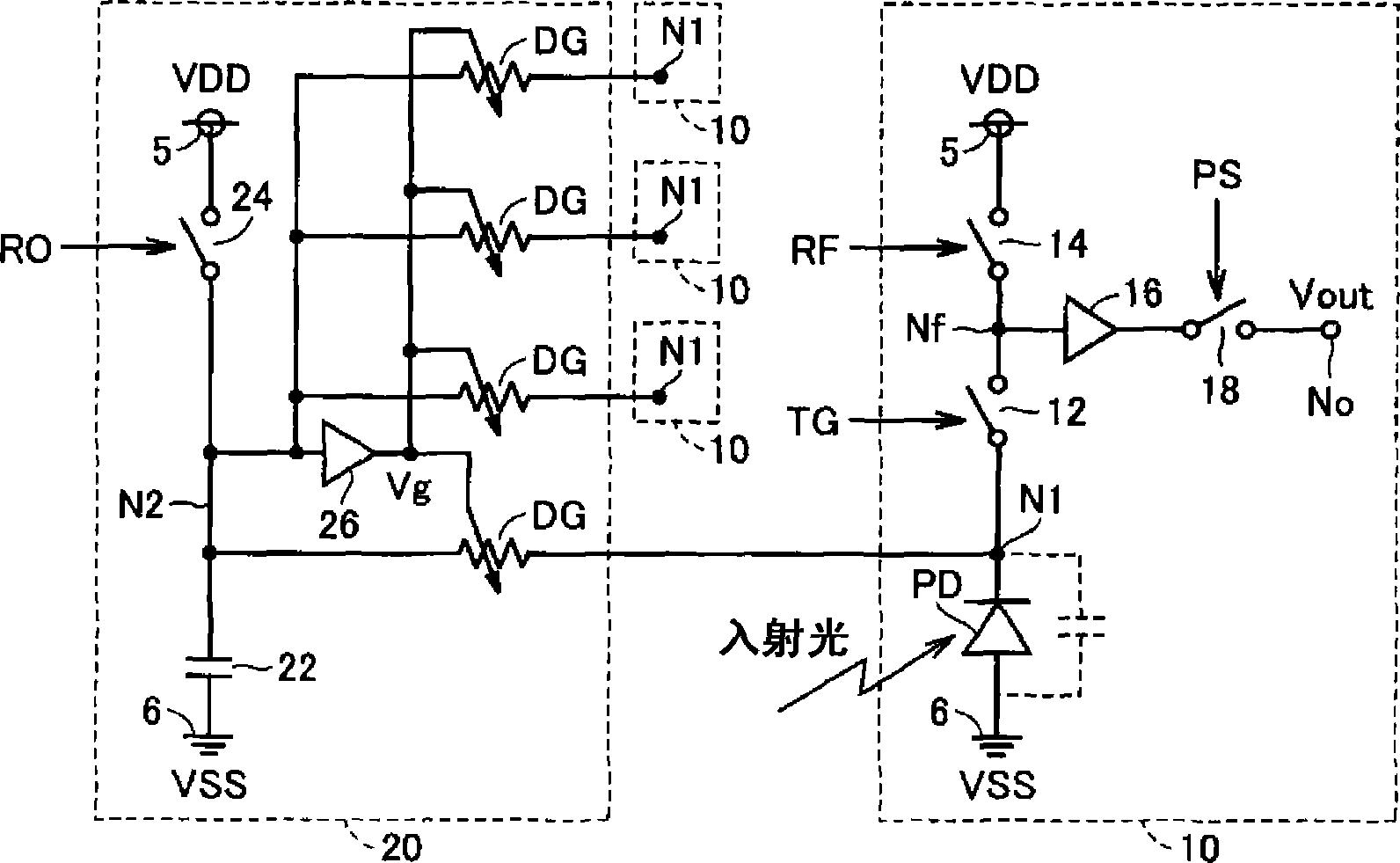
[0046] figure 1 It is a circuit diagram illustrating a schematic configuration of key parts of the semiconductor imaging element according to Embodiment 1 of the present invention.

[0047] refer to figure 1 The pixel circuit 10 has a photodiode PD as a photosensitive detection element, a transmission gate 12 , a reset switch 14 , a voltage amplifier 16 , and a pixel selection switch 18 .

[0048] The reset switch 14 is arranged between the power supply potential node 5 to which the power supply potential VDD is supplied and the node Nf functioning as a floating diffusion, and is turned on and off in accordance with a reset control signal. The transfer gate 12 is connected between the node N1 where signal charges are stored due to the generation of photocurrent of the photodiode PD and the node Nf. The on-off of the transmission gate 12 is controlled by the transmission control signal TG.

[0049] The photodiode PD is arranged between the ground node 6 supplied with the gro...

Embodiment approach 2

[0136] Figure 12 It is a circuit diagram illustrating the configuration of a pixel circuit and an accumulated charge discharge circuit in the semiconductor imaging element according to the second embodiment.

[0137] refer to Figure 12 , In the semiconductor imaging element of Embodiment 2, an accumulated charge discharge circuit 21 is provided instead of the accumulated charge discharge circuit 20 of Embodiment 1.

[0138] The stored charge discharge circuit 21 has figure 1 In the shown stored charge discharge circuit 20 , a photodiode PD# as a “second photodetection element” is arranged between the node N2 and the ground node 6 .

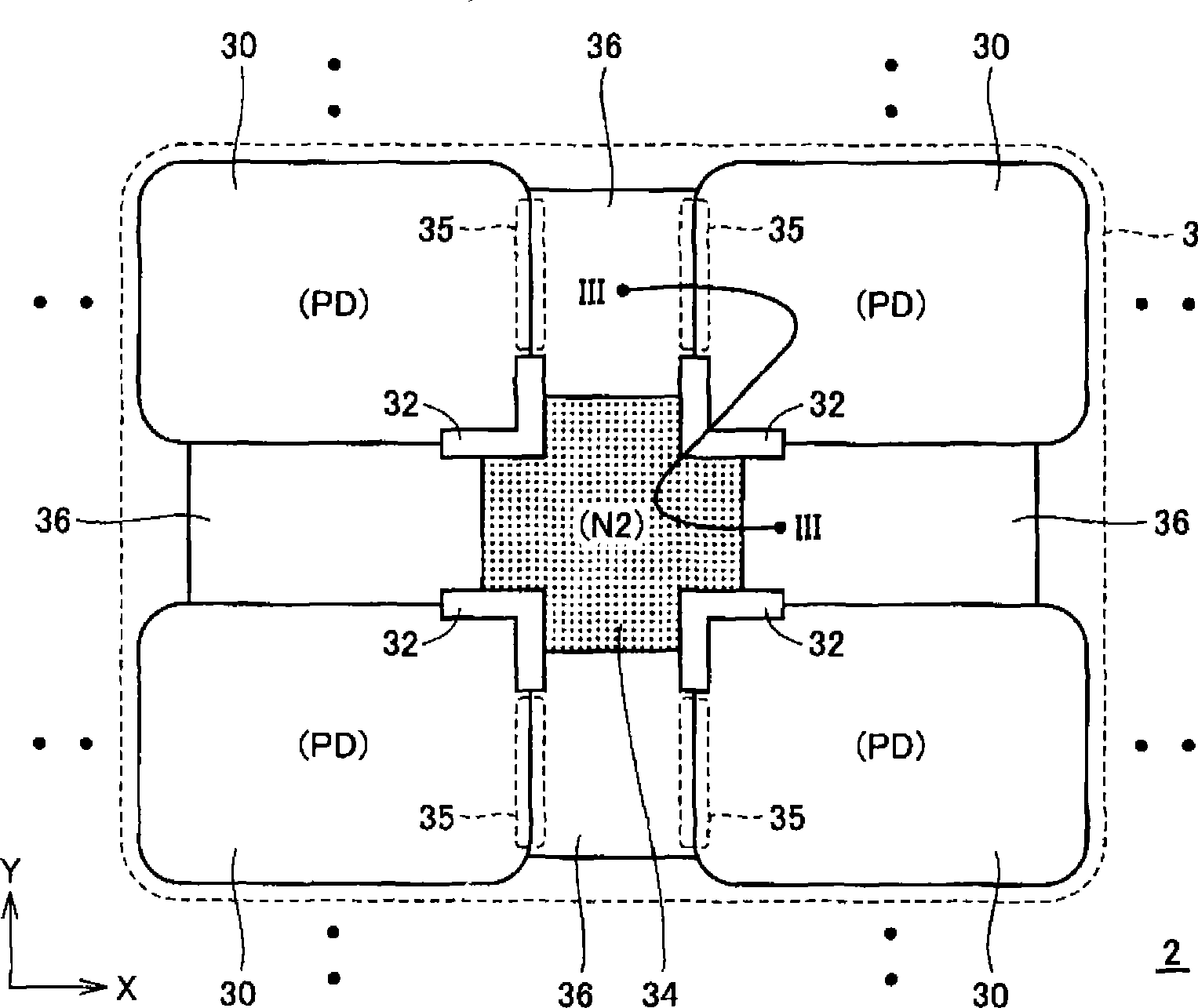
[0139] Figure 13 is shown with image 3 The cross-sectional view of key parts of the stored charge discharge circuit 20 shown corresponds to the cross-sectional view of the structure of key parts of the stored charge discharge circuit 21 . from Figure 13 and image 3 As can be understood by comparison, the stored charge discharge circui...

Embodiment approach 3

[0148] Combining the pixel circuit 10 or 11 and the accumulated charge discharge circuit 20 or 21 as described above constitutes the semiconductor imaging device according to the embodiment of the present invention. Here, Embodiments 1 and 2 exemplify a circuit configuration in which the anode of the photodiode PD is fixed to the ground potential VSS, but a circuit configuration in which the polarity of each circuit is reversed and the cathode of the photodiode PD is fixed to the power supply potential VDD may also be adopted. .

[0149] Figure 14 and Figure 15 Pixel circuits 10 # and 11 # of Embodiment 3 are shown as modified examples in which the polarities of the pixel circuits 10 and 11 are respectively reversed.

[0150] In the pixel circuits 10# and 11#, the cathode of the photodiode PD is connected to the power supply potential node 5. Compared with the pixel circuits 10 and 11, the node N1 is connected to the power supply potential node 5 and the ground node 6 resp...


PUM


Abstract

A signal charge corresponding to an incident light quantity is accumulated in a first node (N1) of each pixel circuit (10). An accumulated charge exhaust circuit (20) includes each of first nodes (N1) of the plurality of pixel circuits (10) belonging to the same pixel group, and a second node (N2) connected through discharge gates (DG) functioning as variable resistance elements. Second node (N2) functions as a floating drain during an ON period of a control switch (24), while accumulating the signal charge overflowing from each pixel circuit (10), in a capacitor (22) during an OFF period of control switch (24) provided at an intermediate timing in one frame period. When the incident light to the pixel group is intense, a resistance value of each discharge gate (DG) is lowered in response to an increase of the signal charge accumulated in capacitor (22), so that the signal charge accumulated in each pixel circuit can be exhausted once at the above intermediate timing.

Description

technical field [0001] The present invention relates to a semiconductor imaging device; more specifically, the present invention relates to a semiconductor imaging device capable of imaging in a large dynamic range even if there is a region with a large brightness difference in the field of view and capable of detecting sufficient contrast in the entire region. Background technique [0002] Starting with video cameras and digital cameras, even mobile phones now have built-in solid-state imaging elements such as CCD (Charge-coupled device) and CMOS (Complementary metal-oxide semiconductor: Complementary Metal-Oxide Semiconductor) imaging elements, so-called semiconductor imaging devices. Sensors (hereinafter also referred to as "semiconductor imaging elements") are widely used as inexpensive and low-power imaging elements. [0003] However, the sensing capability of semiconductor imaging elements is much inferior to thermal visual sensing. Thermal vision can fully detect the...

Claims


Application Information

Patent Timeline
Patent Type & Authority Applications(China)
IPC IPC(8): H04N5/335H01L27/146H04N5/347H04N5/355H04N5/359H04N5/369H04N5/374
CPCH04N5/3745H04N3/155H04N5/37457H01L27/14643H04N5/3559H01L27/14609H01L27/14641H04N25/575H04N25/59H04N25/778H04N25/77
Inventor 广津总吉广津寿一
Owner KENZAN
Why Eureka
Try Eureka