Thin-film solar cell and its production method
A technology of solar cells and thin films, applied in circuits, photovoltaic power generation, electrical components, etc., can solve the problems of low performance and simple structure, and achieve the effect of improving work performance
- Summary
- Abstract
- Description
- Claims
- Application Information
AI Technical Summary
Problems solved by technology
Method used
Image
Examples
Embodiment 1
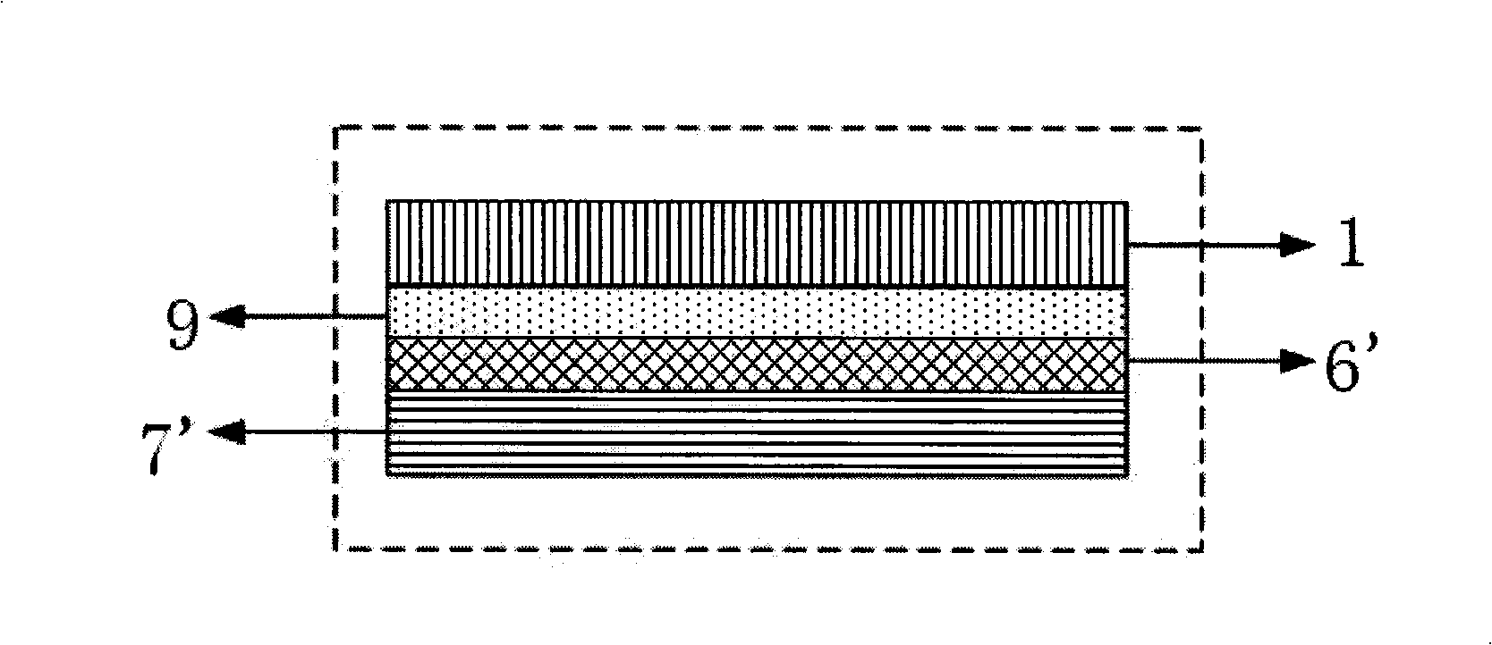
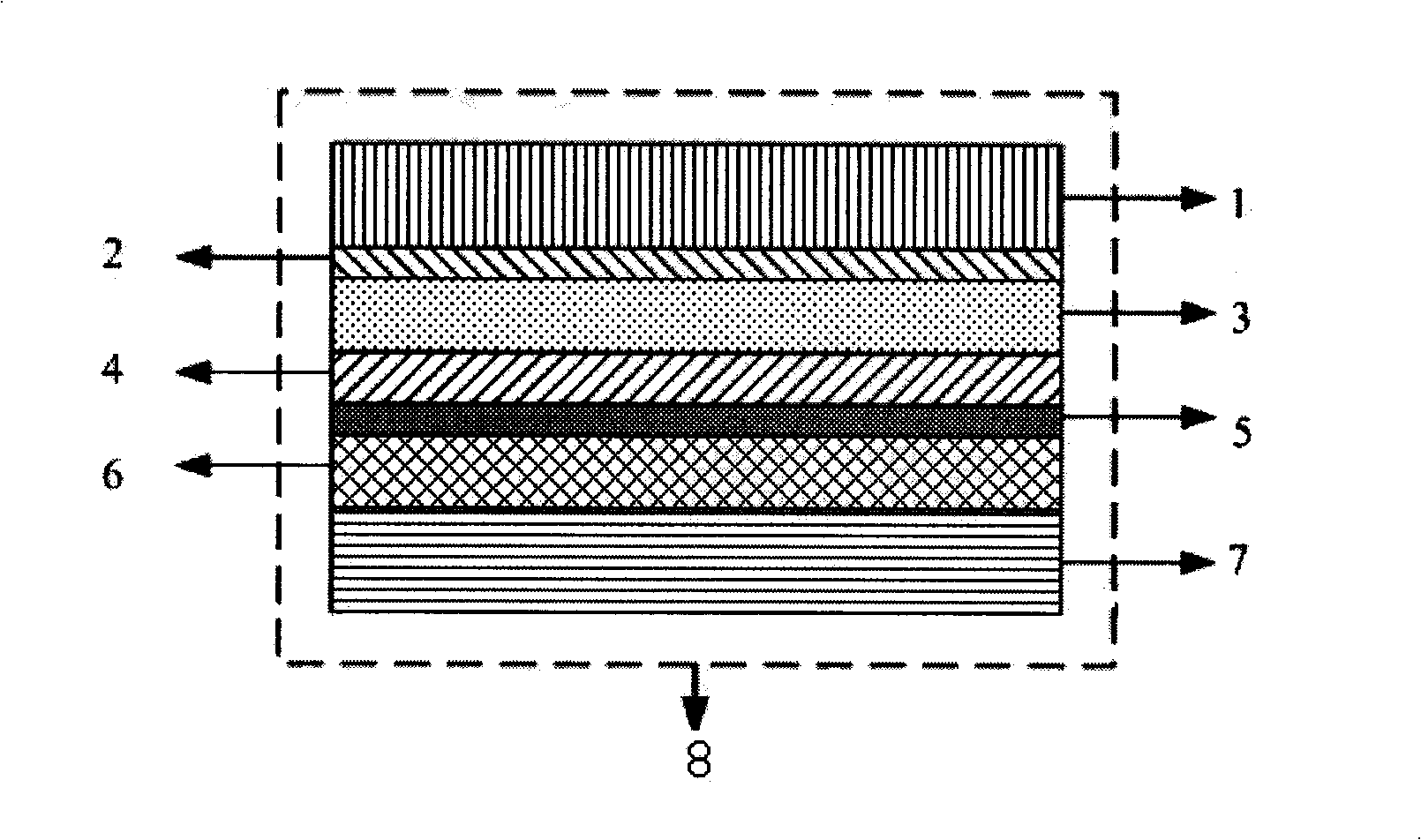
[0039] First, on a glass substrate 1 with an area of 1.1×1.4m and a thickness of 3mm, a tin dioxide thin film with a thickness of about 700nm is made by chemical vapor deposition as a transparent conductive front electrode 2, and a semiconductor layer 3, which is sputtered by magnetron Methods The back electrode 4 zinc oxide film and the functional layer 5 aluminum dioxide film were fabricated to improve the insulation performance. And before the functional layer 5 is plated, a laser etching process is used to achieve such Figure 4 The functional structure shown above is the traditional process of battery production.
[0040] Wherein the semiconductor layer 3 adopts an amorphous photoelectric change structure.
[0041] Next, the edge grinding process is completed, and the thin film structure laminated on the substrate 1 is ground to a width of 8 mm, and the lead wires of the front and rear electrodes are drawn out.
[0042] Next, evenly coat and mix the uncured adhesive l...
PUM
| Property | Measurement | Unit |
|---|---|---|
| Thickness | aaaaa | aaaaa |
| Thickness | aaaaa | aaaaa |
Abstract
Description
Claims
Application Information
 - R&D Engineer
- R&D Manager
- IP Professional
- Industry Leading Data Capabilities
- Powerful AI technology
- Patent DNA Extraction
Browse by: Latest US Patents, China's latest patents, Technical Efficacy Thesaurus, Application Domain, Technology Topic, Popular Technical Reports.
© 2024 PatSnap. All rights reserved.Legal|Privacy policy|Modern Slavery Act Transparency Statement|Sitemap|About US| Contact US: help@patsnap.com


