
Tapping type high-sensitivity SPM feeler based on PVDF and measurement method

A high-sensitivity, probe technology, used in electromagnetic measurement devices, electric/magnetic profile/curvature measurement, etc., can solve the problems of short effective length, limited use range, and vertical resolution can only reach tens of nanometers. Significant effect of aspect ratio, avoidance of additional position detection devices, high-precision non-destructive measurement

Inactive Publication Date: 2011-09-28
HEFEI UNIV OF TECH
View PDF0 Cites 0 Cited by
  • Summary
  • Abstract
  • Description
  • Claims
  • Application Information

AI Technical Summary

Problems solved by technology

[0003] The commonly used stylus profiler is a simple and reliable precision measuring instrument widely used in mechanical surface measurement. Its measurement range can reach tens of millimeters, but its vertical resolution can only reach tens of nanometers, and the measurement process The middle stylus is in continuous contact with the surface to be measured, and the lateral force is large, which is easy to cause scratches on the surface. It is not suitable for the measurement of soft materials and surfaces with steep microstructures.
Although optical measurement systems such as confocal microscopes have the advantage of non-contact measurement, and their highest vertical resolution is close to 10 nanometers, their lateral resolution cannot be improved due to the limitation of the focus spot diameter, and they are not suitable for non-reflective materials Measurement
Although the scanning tunneling microscope (STM) has the advantages of sub-nanometer vertical resolution and non-contact measurement, it cannot be directly applied to insulating materials and materials whose surface is easily oxidized because the measurement current is greatly affected by the conductivity of the measured material. There are also high requirements for the vacuum degree of the measurement environment, so its application range is greatly limited
Although the atomic force microscope (AFM) is suitable for the measurement of various materials and parameters, and has sub-nanometer vertical resolution and nN-level measurement force, most of the probes used are silicon micro-cantilever type, and its effective length Short, tip curvature radius is large, and the cone angle is usually about 30°, which is not suitable for the measurement of large-step microscopic surfaces, and the control of the silicon cantilever used in the probe needs to be realized by additional position detection systems such as optical lever method or optical interference method. , the leaked light generated by the optical detection system not only affects the measurement of the electrical parameters of the semiconductor device, but may also bring interference errors to the surface measurement
Therefore, the structure is complex and difficult to achieve adjustment and detection
Therefore, the existing surface topography measurement system does not have the universality of using

Method used


Image

  • Tapping type high-sensitivity SPM feeler based on PVDF and measurement method
  • Tapping type high-sensitivity SPM feeler based on PVDF and measurement method
  • Tapping type high-sensitivity SPM feeler based on PVDF and measurement method

Examples


Embodiment Construction

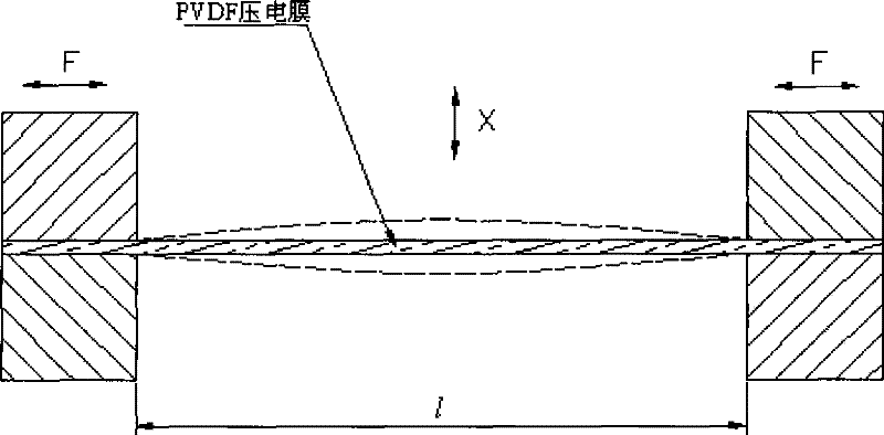
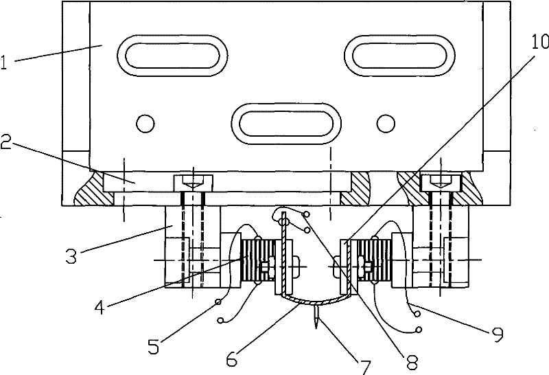
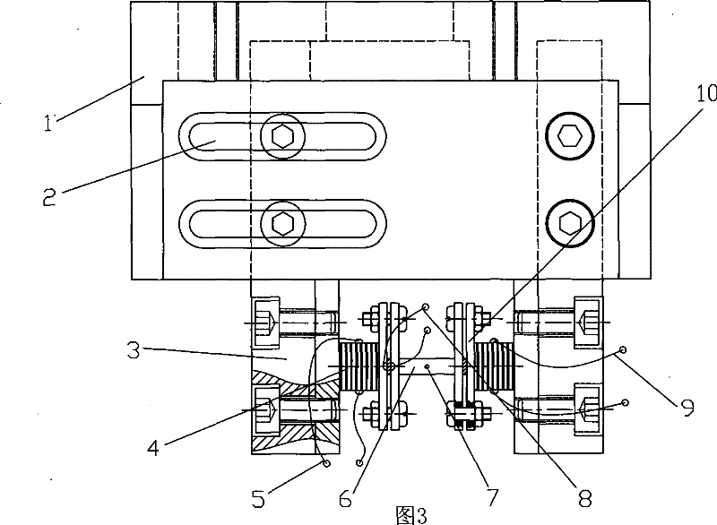
[0019] see figure 1 , figure 2 In this example, the PVDF piezoelectric film is used as the vibrating beam 6, and the tungsten probe is used as the scanning probe 7; The front ends of the piezoelectric actuators 4 on both sides are fixed on the opposite sides, and the rear ends of the piezoelectric actuators 4 on both sides are respectively fixed on the respective cantilever beams 3, and the cantilever beams 3 are suspended on the probe frame 1 at one end; scanning The probe 7 is fixedly arranged at the center of the lower surface of the vibrating beam 6 .

[0020] The measurement method is to apply an AC sinusoidal voltage signal with adjustable amplitude and frequency on the piezoelectric actuators 4 on both sides as the driving signal. The scanning probe 7 vibrates in the vertical direction; the frequency of the driving signal is adjusted so that the vibrating beam 6 is in a near-resonant state; during the scanning process, when the scanning probe 7 has not touched the sa...


PUM


Abstract

The invention relates to a PVDF-based tapping-mode high-sensitivity SPM measuring head and a measuring method thereof. The PVDF-based tapping-mode high-sensitivity SPM measuring head is characterized in that a PVDF piezoelectric membrane is taken as a vibrating beam and a tungsten probe is taken as scanning probe; the vibrating beam is set to be a simply supported beam with bended radian; the left end and the right end of the vibrating beam are fixed on front ends of oppositely arranged piezoelectric drivers on both sides through clamping structures respectively; rear ends of the piezoelectric drivers on both sides are fixed on respective cantilever beams respectively; one end of each of the cantilever beams is suspended on a measuring head holder; and the scanning probe is fixed on a center position on the lower surface of the vibrating beam. The measuring method takes the variation of electric charges outputted by the vibrating beam to represent the amplitude variation of the vibrating beam caused by a micrometering force, and performs multipoint micrometering force tapping scanning on a surface to be measured to realize measurement of the surface of a sample. The PVDF-based tapping-mode high-sensitivity SPM measuring head and the measuring method can realize high spatial resolution and low measuring force, are suitable for various materials, and can measure under air environment.

Description

technical field [0001] The invention relates to a nanometer measurement device, more specifically a measuring head that can be used to form a scanning probe microscope system, so that the system can realize the feedback control of the nanometer resolution in the vertical direction in the measurement of the nanometer microscopic shape; it can form a micro-nano three-dimensional The nano-positioning probe of the coordinate measuring machine realizes the nano-positioning of the probe of the three-coordinate measuring machine; it can be used to form a scanning probe microscope system to realize the surface characteristics of soft and fragile samples (such as the surface of biological materials such as protein molecules) and steep steps Samples (such as semiconductor silicon micro-devices, micro-electro-mechanical devices, etc.) for non-destructive micro-surface topography measurement at nanoscale resolution; Measurement of micromechanical parts. Background technique [0002] In...

Claims


Application Information

Patent Timeline
Patent Type & Authority Patents(China)
IPC IPC(8): G01B7/28
Inventor 黄强先侯茂盛杨朋桢罗涛张瑜
Owner HEFEI UNIV OF TECH
Learn More