Non-volatile memory and preparation thereof

A non-volatile, manufacturing method technology, applied in semiconductor/solid-state device manufacturing, electrical solid-state devices, semiconductor devices, etc., can solve the problem that the coupling rate cannot be greatly improved

Active Publication Date: 2009-03-18
NAN YA TECH
View PDF0 Cites 4 Cited by
  • Summary
  • Abstract
  • Description
  • Claims
  • Application Information

AI Technical Summary

Problems solved by technology

[0006] However, in the above-mentioned non-volatile memory, although the T-shaped control gate is used to increase the coupling rate with the floating gate, the coupling rate cannot be greatly increased to adapt to future technological developments.

Method used


Image

  • Non-volatile memory and preparation thereof
  • Non-volatile memory and preparation thereof
  • Non-volatile memory and preparation thereof

Examples


Embodiment Construction

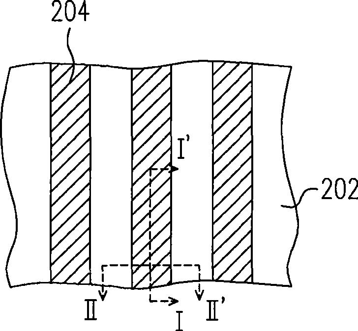
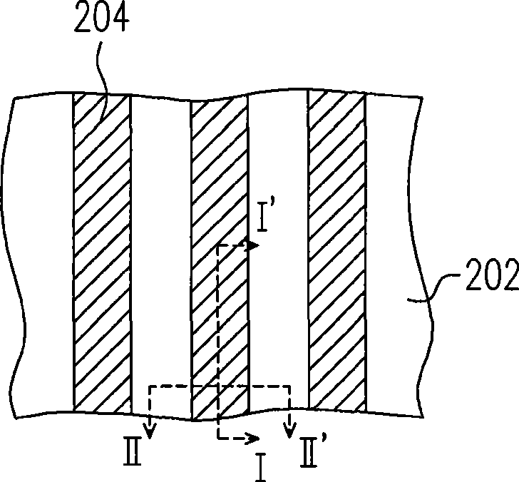
[0044] Figure 2A to Figure 2F It is a top view of the fabrication process of the non-volatile memory according to the embodiment of the present invention. Figure 3A to Figure 3F for along Figure 2A to Figure 2F The cross-sectional view of the fabrication process of the non-volatile memory shown in the I-I' cross-section. Figure 4A to Figure 4F for the along Figure 2A to Figure 2F The cross-sectional view of the fabrication process of the non-volatile memory shown in the II-II' section.

[0045] First, please also refer to Figure 2A , Figure 3A and Figure 4A , providing a substrate 200. The substrate 200 is, for example, a silicon substrate. Then, a dielectric layer (not shown) and a conductive layer (not shown) are sequentially formed on the substrate 200 . The material of the dielectric layer is, for example, oxide, and its formation method is, for example, thermal oxidation. The material of the conductor layer is, for example, polysilicon, and its formation ...


PUM


Abstract

The invention relates to a nonvolatile memory, which comprises a gate structure and a source electrode / drain region, wherein the gate structure is arranged on a base, and comprises floating gates, a tunneling dielectric layer, a control gate and a gate dielectric layer, wherein the floating gates are arranged on the base, the tunneling dielectric layer is arranged between each floating gate and the base, the control gate is arranged on the base between the pair of the floating gates, and covers the top surface and at least side walls of each floating gate, the gate dielectric layer is arranged between the control gate and each floating gate and between the control gate and the tunneling dielectric layer, and is arranged between the control gate and the base, and the source electrode-drain region is arranged in the base on the two sides of the gate structure. Therefore the invention increases the covered area of the floating gate by the control gate, and further increases the coupling rate between the control gate and the floating gate.

Description

technical field [0001] The present invention relates to a memory and its manufacturing method, and in particular to a non-volatile memory (non-volatile memory) and its manufacturing method. Background technique [0002] Non-volatile memory is widely used in personal computers and electronic devices because it can store, read, and erase data multiple times, and the stored data will not disappear after power failure. However, with the miniaturization of semiconductor components, the size of the memory is also reduced along with the reduction of the line width, which makes the gap between the control gate (control gate) and the floating gate (floating gate) in the non-volatile memory Coupling ratio (coupling ratio) is greatly reduced. [0003] Therefore, in order to increase the coupling rate between the control gate and the floating gate, the coupling rate is usually increased by increasing the coverage area between the control gate and the floating gate. [0004] figure 1 ...

Claims


Application Information

Patent Timeline
Patent Type & Authority Applications(China)
IPC IPC(8): H01L21/8247H01L21/336H01L21/28H01L27/115H01L29/788H01L29/423
Inventor 廖伟明张明成黄建章
Owner NAN YA TECH
Why Eureka
Try Eureka