Apparatus used for debugging programmable chip and field programmable gate array chip

A chip and debugging host technology, applied in the field of hardware programmable, can solve the problems of high cost, difficulty in changing the circuit in seconds, and increase of product cost

Inactive Publication Date: 2009-02-18
BEIJING XINWANG RUIJIE NETWORK TECH CO LTD
View PDF2 Cites 27 Cited by
  • Summary
  • Abstract
  • Description
  • Claims
  • Application Information

AI Technical Summary

Problems solved by technology

[0014] ① The rationality of the establishment of the simulation debugging platform (TestBenches) cannot be guaranteed
[0017] ②The time for simulation debugging is limited
However, 100 picosecond-level calculations will consume a lot of memory storage resources and CPU computing resources. Therefore, it is difficult to reflect the second-level changes in the circuit through simulation tools.
[0020] ③The authenticity of the simulation is limited
Moreover, this configuration architecture uses DSP / MPU chips, which increases product costs, especially in small and medium-sized FPGA applications.

Method used


Image

  • Apparatus used for debugging programmable chip and field programmable gate array chip
  • Apparatus used for debugging programmable chip and field programmable gate array chip
  • Apparatus used for debugging programmable chip and field programmable gate array chip

Examples


Embodiment Construction

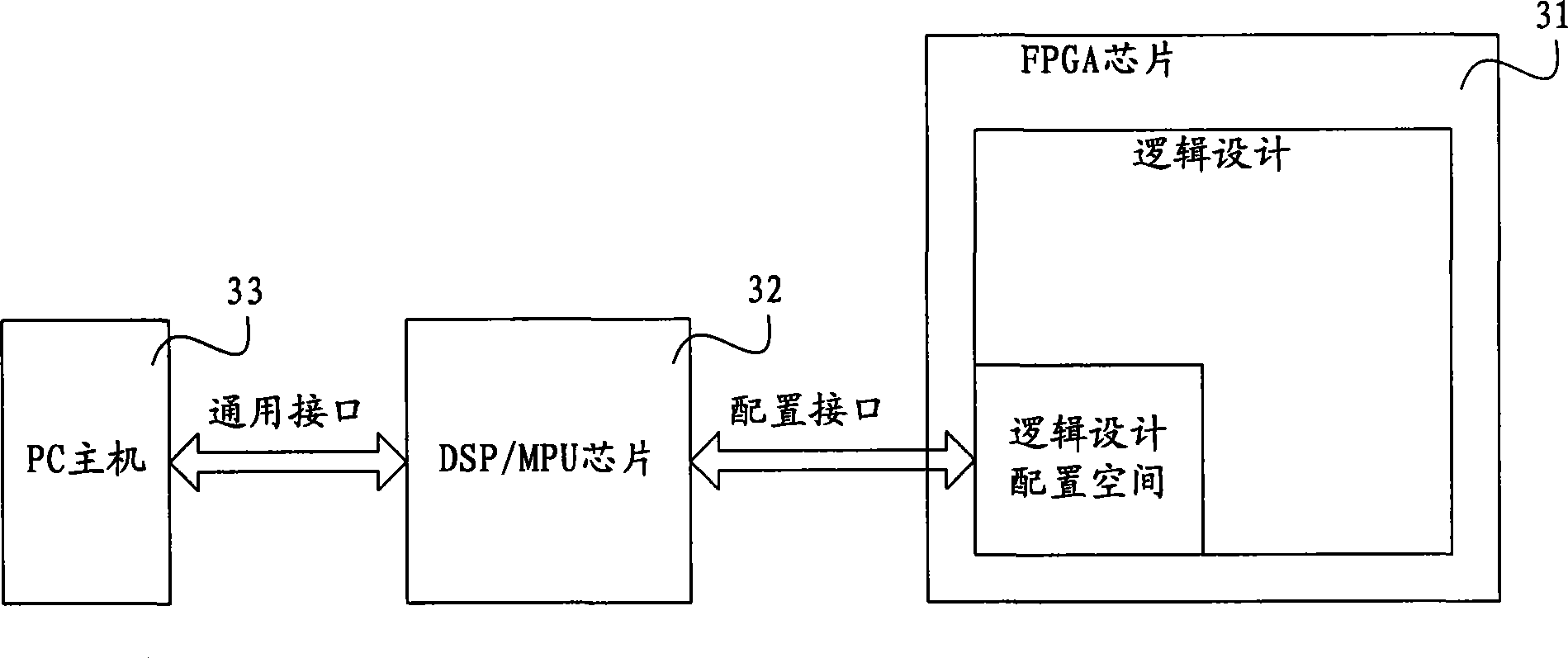
[0072] Figure 4It is a schematic structural diagram of Embodiment 1 of the device for debugging a programmable chip of the present invention. The device for debugging the programmable chip includes: a physical layer 41 , a decoding operation module 42 , an encoding operation module 43 , a command operation module 44 and a debugging interface 45 . The physical layer 41 is connected with the debugging host 46 outside the FPGA chip, and is used for carrying out command data interaction with the debugging host 46; the decoding operation module 42 is used for decoding the command data received by the physical layer 41; The encoding operation module 43 is used to combine the command information containing the signal state information into command data, and send it to the debugging host 46 through the physical layer 41; the command operation module 44 is used to decode according to the decoding operation module 42 to obtain The command information of the command information is used...


PUM


Abstract

The invention relates to a device for debugging a programmable chip and an FPGA (field programmable gate array) chip. The device comprises: a physics layer which is connected with a debugging main computer outside the programmable chip, a decoding operation module, an encoding operation module, a command operation module, and a debugging port which is used for providing the interface that can obtain signal status information for the command operation module. The FPGA (field programmable gate array) chip comprises a device which is used for debugging the programmable chip and the debugging port. The invention also relates to a complex PLD (programmable logic device) chip, which comprises the device that is used for debugging the programmable chip and the debugging port. In the technical proposal, the device for debugging the programmable chip has simple structure without consuming hardware source, greatly reduces the complexity, and is convenient for realization in low-end programmable chip, and greatly improves the universality of the debugging device.

Description

technical field [0001] The present invention relates to hardware programmable technology, in particular to a device for debugging a programmable chip, a Field Programmable Gate Array (Field Programmable Gate Array, FPGA for short) chip, and a Complex Programmable Logic Device (CPLD for short). )chip. Background technique [0002] FPGA is a new high-performance programmable chip with high integration, suitable for high-speed, high-density high-end digital logic circuit design. The FPGA has an internal programmable (Programmable) circuit function, that is, it can flexibly implement extremely complex circuit functions inside it through a hardware description language (Hardware Description Language, HDL for short) and a dedicated design tool. [0003] figure 1 Flowchart for FPGA development and design. "Functional Requirements" in the figure proposes the circuit functional requirements that the FPGA chip should complete. [0004] In the first stage of design11, FPGA designer...

Claims


Application Information

Patent Timeline
Patent Type & Authority Applications(China)
IPC IPC(8): G01R31/3185G01R31/317G06F17/50
CPCH03K19/17732H03K19/17764
Inventor 彭鼎祥彭少宁
Owner BEIJING XINWANG RUIJIE NETWORK TECH CO LTD
Why Eureka
Try Eureka