LED unit and LED apparatus
A technology for an LED device and a control unit, which is applied to lighting devices, components of lighting devices, circuit layout, etc., can solve the problems of increased PCB board area, difficulty in making LED devices into transparent products, and unsightly viewing surfaces.
- Summary
- Abstract
- Description
- Claims
- Application Information
AI Technical Summary
Problems solved by technology
Method used
Image
Examples
Embodiment 1
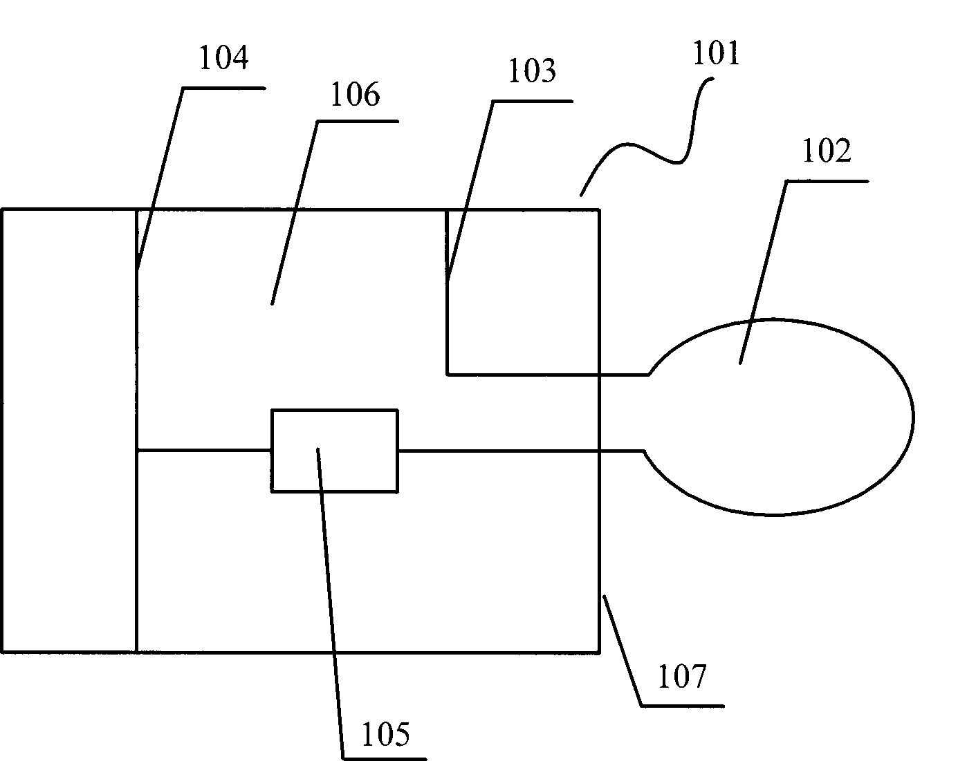
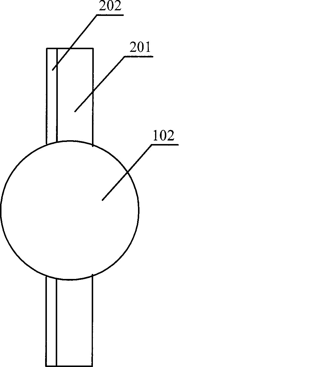
[0039] Such as figure 1 and figure 2 As shown, the LED unit of the present invention includes a PCB board 101 and an LED light emitting diode 102 . The PCB board 101 includes an insulating substrate 201 and a conductive pattern layer 202. In order to make the lateral footprint of the LED unit smaller, the light-emitting surface of the LED light-emitting diode 102 is arranged on the same side 107 of the PCB board 101; in the present invention, the LED light-emitting diode The light-emitting surface of a certain LED light-emitting diode includes each light-transmitting surface except the base; at the same time, it is better to make the main light-emitting direction of the LED light-emitting diode 102 face away from the side.
[0040] For example, the LED light-emitting diode 102 can be installed and fixed on the edge of the side 106 of the PCB 101 close to the side, and the light-emitting surface is arranged on the same side 107 of the PCB 101 . In this way, the LED light-emi...
Embodiment 2
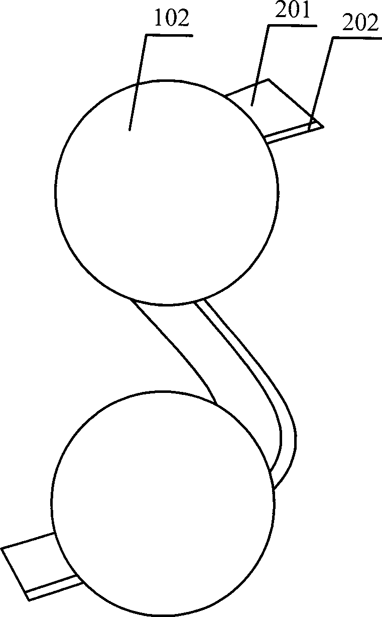
[0043] Such as image 3 As shown, the LED unit of the present invention includes a PCB board 101 and an LED light-emitting diode 102. The PCB board 101 is a flexible PCB board, and the flexible PCB board is made of soft layered plastic or other soft insulating materials. The finished parts can be bent and stretched, and can be bent and shaped according to installation requirements during use.
[0044] The flexible PCB 101 includes an insulating substrate 201 and a conductive pattern layer 202 , and the light emitting surfaces of the LED light emitting diodes 102 are arranged on the same side of the insulating substrate 201 . The LED unit composed of a flexible PCB board can be bent and shaped arbitrarily, such as image 3 The S shape; when not in use, the product can also be bent and folded, making storage and transportation very convenient.
Embodiment 3
[0046] On the basis of Embodiment 1 and / or Embodiment 2, the PCB board of the present invention can also be a PCB board with more than 2 layers, and the multi-layer PCB board can meet the requirements of installing enough electronic components in a PCB board with limited horizontal space And electronic circuits, and the multi-layer PCB board has a stronger load-bearing capacity, and can install LED light-emitting diodes more stably. The preferred solution of the present invention is a PCB board with 2 to 10 layers, such as a PCB board with 4, 5, 6, 7, and 8 layers. Each PCB board includes an insulating substrate and a conductive pattern layer printed on the insulating substrate. A conductive graphic layer is printed on one surface of the insulating substrate, which is a single-sided PCB layer; a conductive graphic layer is printed on both surfaces of the insulating substrate, which is a double-sided PCB layer. The above-mentioned 2 to 10-layer PCB board can be composed of onl...
PUM
 Abstract
Description
Claims
Application Information
 - R&D
- Intellectual Property
- Life Sciences
- Materials
- Tech Scout
- Unparalleled Data Quality
- Higher Quality Content
- 60% Fewer Hallucinations
Browse by: Latest US Patents, China's latest patents, Technical Efficacy Thesaurus, Application Domain, Technology Topic, Popular Technical Reports.
© 2025 PatSnap. All rights reserved.Legal|Privacy policy|Modern Slavery Act Transparency Statement|Sitemap|About US| Contact US: help@patsnap.com


