


Quick Research
Generate reliable direction feasibility study reports for your R&D in just a few steps.

Technical Q&A
Discover and master advanced knowledge NOW. Basics, ideas, possibilities, all at once.

Find Solutions
As an expert in R&D theories, this can generate solutions to your technical problems instantly.

Evaluate Feasibility
Analyze your overall solution with one click, know your potential R&D risks in advance.

Monitor Landscape
Get weekly tech updates, stay abreast of the latest tech innovations and key insights.
Semiconductor device
A semiconductor, integrated technology, applied in the direction of semiconductor devices, semiconductor/solid-state device components, electric solid-state devices, etc., can solve the problems of large copper ratio, reduced rigidity of heat sink, inability to miniaturize semiconductor devices, lightweight and low cost, etc. Achieve stable performance and suppress thermal resistance
- Summary
- Abstract
- Description
- Claims
- Application Information
AI Technical Summary
Problems solved by technology
Method used
Image


Examples
no. 1 approach
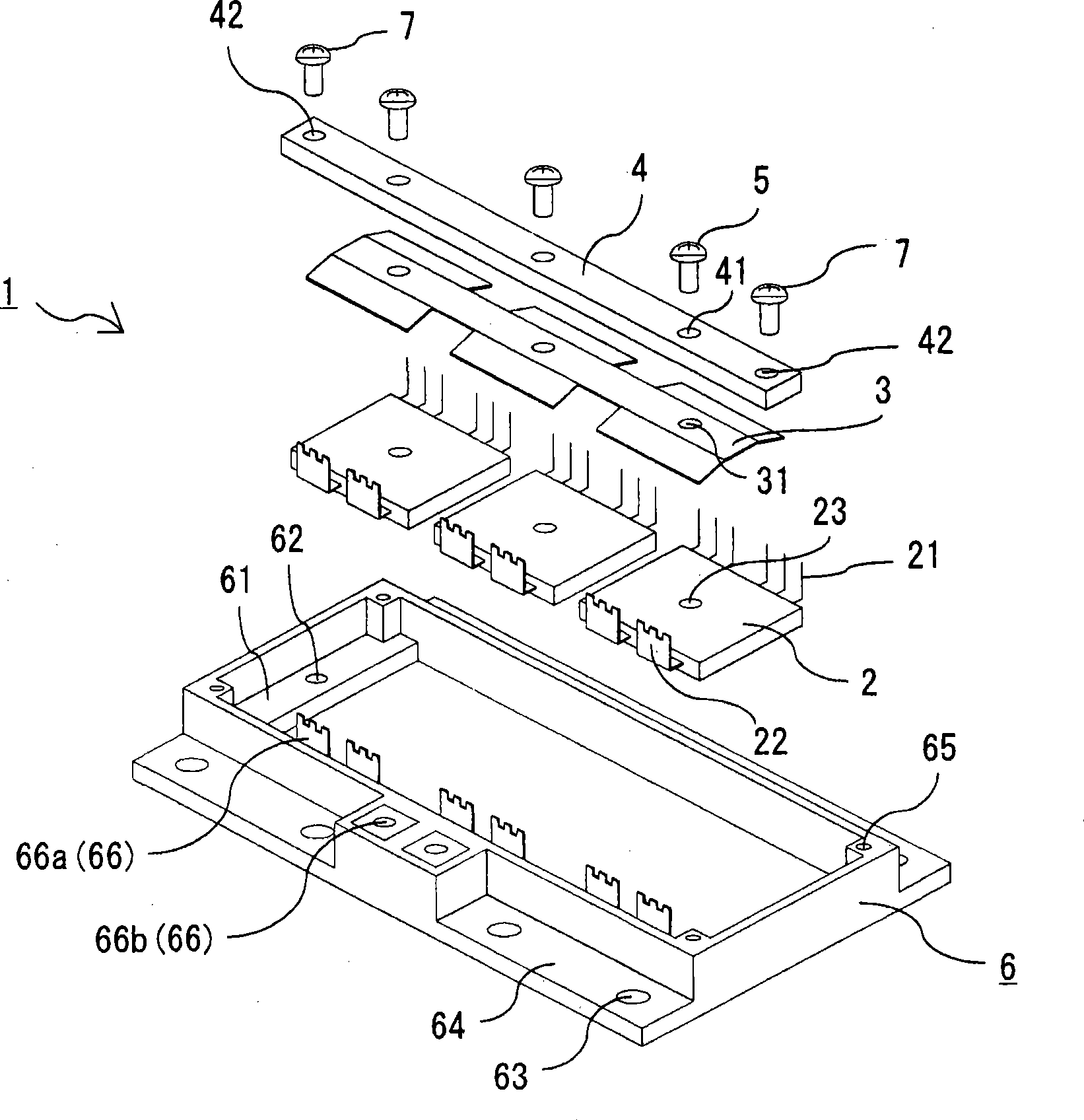
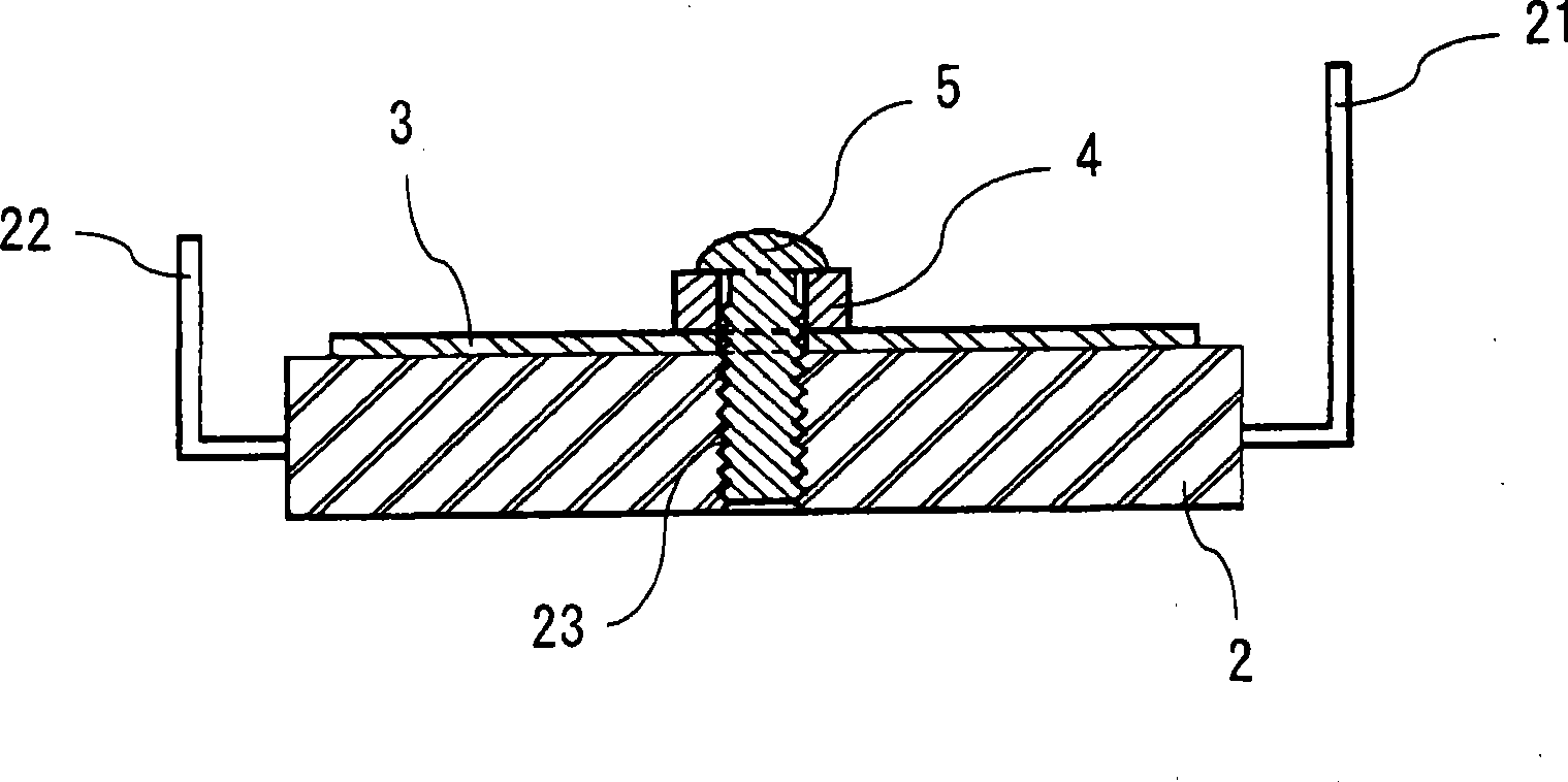
[0021] figure 1 It is an exploded perspective view showing the configuration of the semiconductor device according to the first embodiment of the present invention. figure 2 it means assembled figure 1 A perspective view of the state of the semiconductor device. image 3 Yes figure 2 A partial cross-sectional view of the semiconductor device is shown, and the frame portion is omitted. Figure 4 It is to fix the cooling part and the control part on the figure 2 A schematic diagram of an example of a semiconductor device.
[0022] exist Figure 1 to Figure 3 Among them, the semiconductor device 1 includes: a semiconductor module 2 in which a semiconductor element is sealed with resin; a reinforcing beam 4 fixed to the upper surface of the semiconductor module 2 by a leaf spring 3; The frame portions 6 at both ends of the reinforcing beam 4 are installed and fixed.
[0023] The semiconductor module 2 has a control terminal 21 connected to a control unit described later,...
no. 2 approach
[0048] In the first embodiment, the frame portion 6 is formed of a synthetic resin material, but in the second embodiment, the frame portion is formed of a metal having high rigidity.
[0049] Figure 5 It is an exploded perspective view showing the configuration of the semiconductor device according to the second embodiment of the present invention. Image 6 is assembled Figure 5 A perspective view of the state of the semiconductor device. In addition, the same code|symbol is attached to the same part as 1st Embodiment, and description is abbreviate|omitted.
[0050] exist Figure 5 , Image 6 Among them, the frame portion 6 is formed of, for example, a metal material with high rigidity such as iron, aluminum, and magnesium, and can be manufactured by casting, die casting, or the like. Since the frame portion 6 itself is formed of a conductive material, the structure of the first embodiment, that is, insert molding of the bus bar as the conductive portion, exposed conne...
no. 3 approach
[0055] In the first and second embodiments, the frame portion and the reinforcing beam are formed as separate members and fixed with screws or the like, but in the third embodiment, the frame portion and the reinforcing beam are integrally formed. Further, the material of the frame portion may be a synthetic resin material as in the first embodiment, or a metal material as in the second embodiment, according to the purpose, but a case where a metal material is used will be described in the third embodiment.
[0056] Figure 7 It is an exploded perspective view of the configuration of the semiconductor device according to the third embodiment of the present invention. Figure 8 is assembled Figure 7 A perspective view of the state of the semiconductor device. In addition, the same code|symbol is attached to the same part as 1st Embodiment, and description is abbreviate|omitted.
[0057] like Figure 7 , Figure 8 As shown, the semiconductor module 2 and the leaf spring 30...
PUM
 Abstract
Description
Claims
Application Information
 - R&D Engineer
- R&D Manager
- IP Professional
- Industry Leading Data Capabilities
- Powerful AI technology
- Patent DNA Extraction
Browse by: Latest US Patents, China's latest patents, Technical Efficacy Thesaurus, Application Domain, Technology Topic, Popular Technical Reports.
© 2024 PatSnap. All rights reserved.Legal|Privacy policy|Modern Slavery Act Transparency Statement|Sitemap|About US| Contact US: help@patsnap.com