Large-scale preparation method of hyperfine nanostructure and use thereof
A nano-structure and ultra-fine technology, which is applied in the field of preparation of ultra-fine nano-structures, achieves the effects of high repeatability, easy automatic control, and easy damage
- Summary
- Abstract
- Description
- Claims
- Application Information
AI Technical Summary
Problems solved by technology
Method used
Image
Examples
Embodiment 1
[0037] Embodiment 1, processing ultra-fine nanopores on zinc oxide nanowires / nanorods
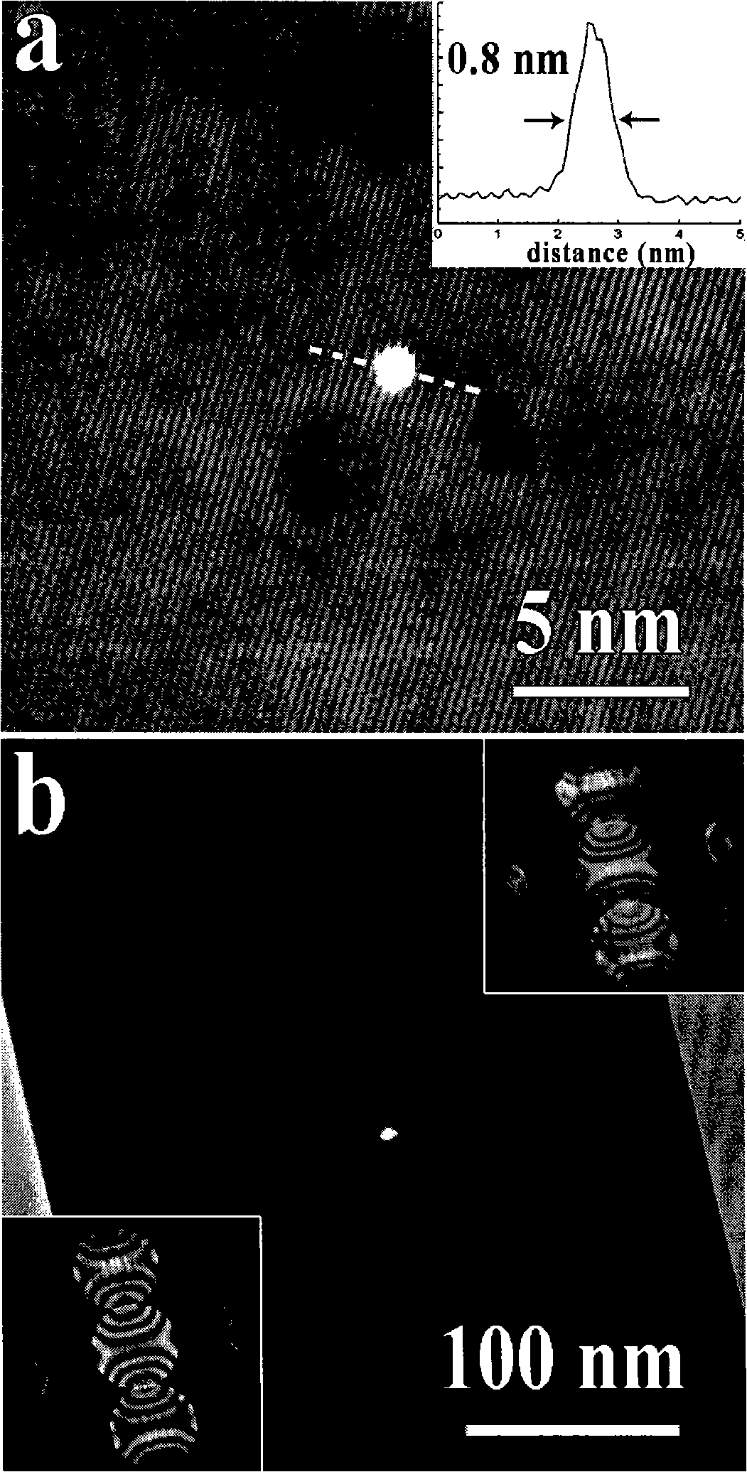
[0038] like figure 1 As shown in (a), the zinc oxide nanowire diameter is 40 nanometers, the exposure time is 10 seconds, the electron beam spot diameter is 1 nanometer, and the nanopore diameter is 0.8 nanometers.
[0039] (b) In the figure, the diameter of the ZnO nanorod is 300 nm, the exposure time is 15 minutes, the diameter of the electron beam spot is about 6 nm, and the diameter of the nanopore is about 5 nm. In addition, the upper right corner is the converging beam diffraction pattern obtained from the experiment, and the lower left corner is the converging beam diffraction pattern obtained by calculation, from which the thickness of the nanorods can be determined.
Embodiment 2
[0040] Embodiment 2, ultra-fine nanopores processed on different materials
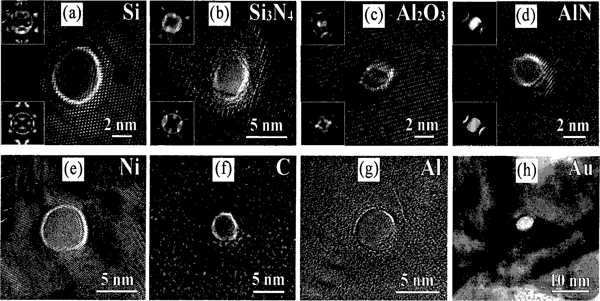
[0041] like figure 2 As shown, (a) is a nanohole processed on a Si[110] film with a thickness of 160 nm. The exposure time is 60 seconds, the diameter of the electron beam spot is 9 nm, and the diameter of the nanopore is 5 nm.
[0042] (b) The picture shows Si at 100 nm thick 3 N4 The nanohole processed on the nanowire, the exposure time is 200 seconds, the diameter of the electron beam spot is 9 nanometers, and the diameter of the nanohole is 4 nanometers.
[0043] (c) Pictured in 95nm Al 2 o 3 For the nanoholes processed on the film, the exposure time is 10 seconds, the diameter of the electron beam spot is 3 nanometers, and the diameter of the nanopores is 3 nanometers.
[0044] (d) The picture shows nanoholes fabricated on 80 nm thick AlN[141] nanorods, with an exposure time of 100 s, an electron beam spot diameter of 3 nm, and a nanopore diameter of 2.5 nm.
[0045] (e) The picture shows n...
Embodiment 3
[0049] Embodiment 3, ultrafine nanohole arrays and nanograting slits processed on zinc oxide nanowires and nanofilms
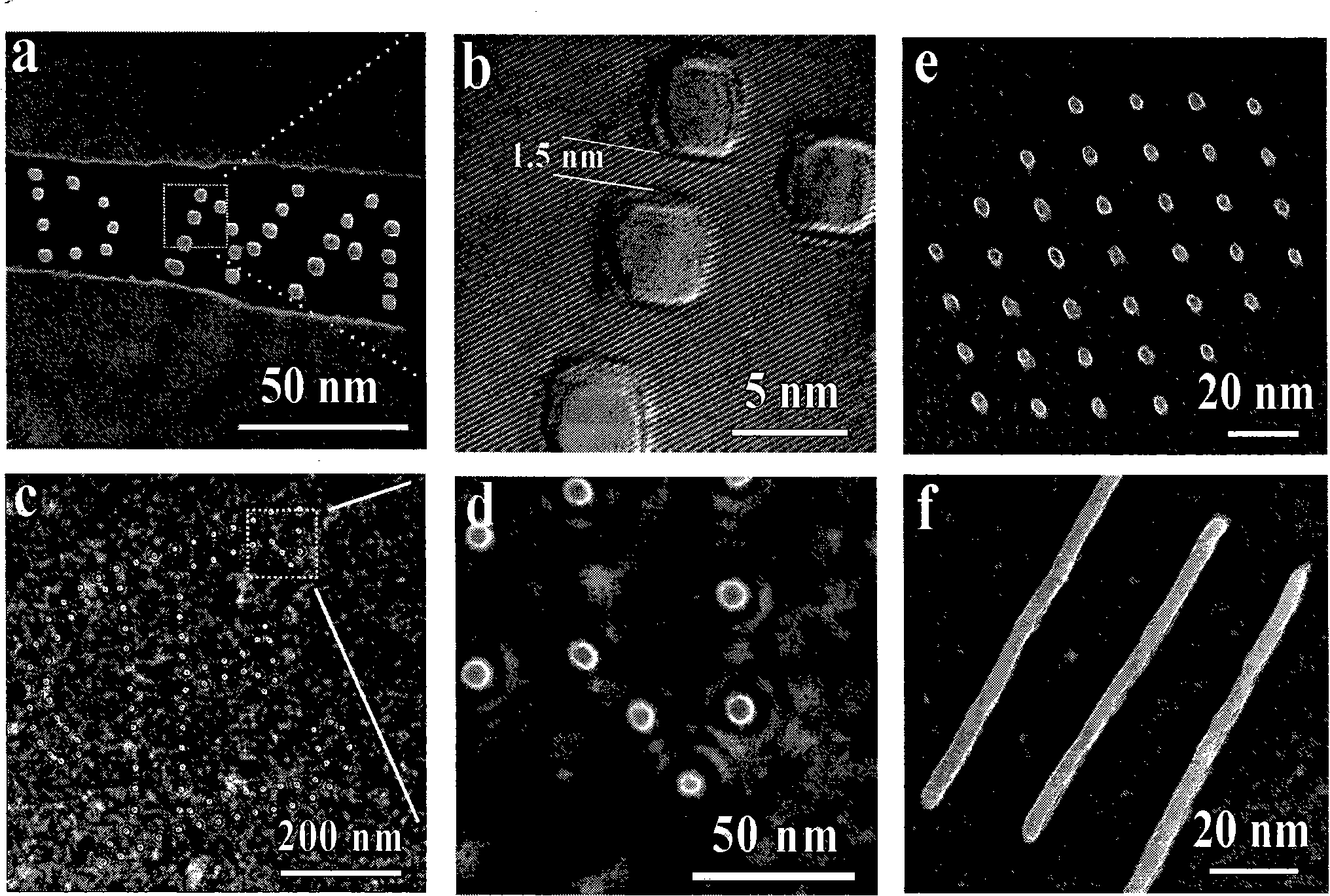
[0050] like image 3 As shown, (a) is an ultra-fine nanohole array processed on a zinc oxide nanowire, the exposure time is 20 seconds, the diameter of the electron beam spot is 3 nanometers, and the diameter of the nanohole is 3 nanometers. (b) is a high-resolution image of (a), with nanopore spacing as small as 1.5 nm.
[0051] (c) The picture shows the nanohole array processed on the 30 nm thick nickel film, the exposure time is 20 seconds, the diameter of the electron beam spot is 5 nm, and the diameter of the nanohole is 6 nm. (d) is a magnified image of (c), and the Fresnel diffraction rings around the hole are clearly visible.
[0052] Figures (e) and (f) are nanohole arrays and nanograting slits processed on a 100 nm thick ZnO film, respectively. Wherein, the diameter of the nanohole is 3 nanometers, and the distance between the nanoholes is 15 nano...
PUM
 Abstract
Description
Claims
Application Information
 - Generate Ideas
- Intellectual Property
- Life Sciences
- Materials
- Tech Scout
- Unparalleled Data Quality
- Higher Quality Content
- 60% Fewer Hallucinations
Browse by: Latest US Patents, China's latest patents, Technical Efficacy Thesaurus, Application Domain, Technology Topic, Popular Technical Reports.
© 2025 PatSnap. All rights reserved.Legal|Privacy policy|Modern Slavery Act Transparency Statement|Sitemap|About US| Contact US: help@patsnap.com


