
Method for forming elementary cell and crystal round with epitaxial slice

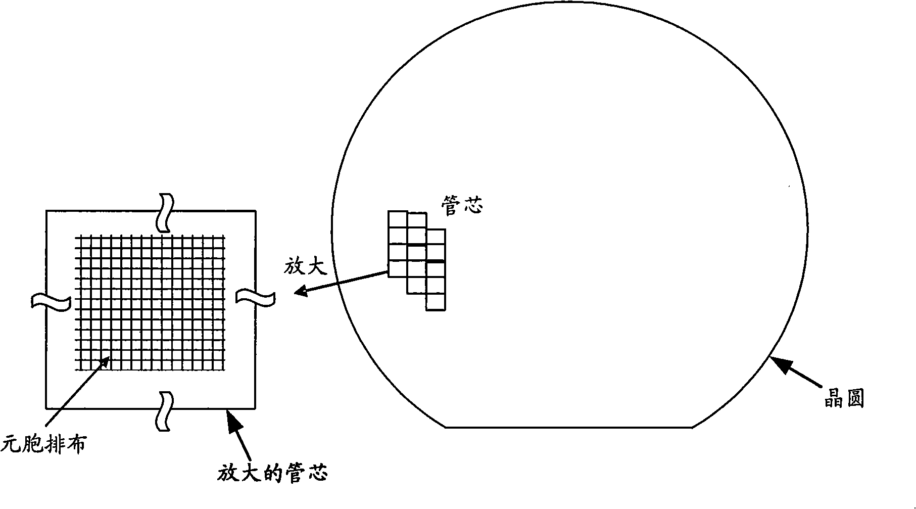
A technology of epitaxial wafers and cells, which is applied in the direction of electrical components, semiconductor/solid-state device manufacturing, circuits, etc., can solve the problem of large source-drain on-resistance, and achieve the effect of reducing source-drain on-resistance

Inactive Publication Date: 2009-01-21
PEKING UNIV FOUNDER GRP CO LTD +1
View PDF0 Cites 0 Cited by
  • Summary
  • Abstract
  • Description
  • Claims
  • Application Information

AI Technical Summary

Problems solved by technology

[0006] Embodiments of the present invention provide a method for forming cells and a wafer with epitaxial wafers, which are used to solve the problem of large source-drain on-resistance in the effective die area of ​​existing semiconductor devices

Method used


Image

  • Method for forming elementary cell and crystal round with epitaxial slice
  • Method for forming elementary cell and crystal round with epitaxial slice
  • Method for forming elementary cell and crystal round with epitaxial slice

Examples


Embodiment Construction

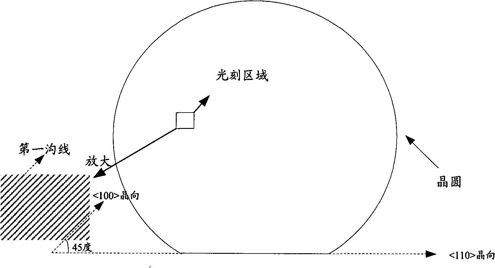
[0017] Embodiments of the present invention provide a method for forming cells and a wafer with epitaxial wafers. Utilize the method of the present invention to print on the surface of the epitaxial wafer in which the main flat side is located in the crystal direction, there are two opposite sides forming an angle of 45 degrees with the crystal direction. This cell unit The source-drain on-resistance on the area is smaller than the source-drain on-resistance of the square cell whose bottom side is parallel to the main flat edge of the epitaxial wafer, thereby reducing the source-drain on-resistance in the effective die area of ​​the semiconductor device and improving the semiconductor performance. The performance of devices (such as DMOS devices, IGBT devices).

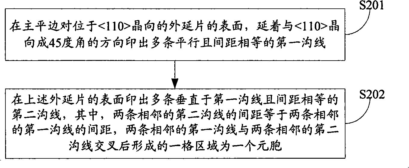
[0018] refer to figure 2 As shown, the method for forming cells on an epitaxial wafer includes the following steps:

[0019] S201. On the surface of the epitaxial wafer located in the crystal direction on the ma...


PUM


Abstract

The invention discloses a method for forming a cell and a wafer with an epitaxial slice, which are used for solving the problem that a source-drain on-state resistance which is arranged in an effective tube core area of an existing semi-conductor component is bigger. The method comprises the following steps: printing a plurality of first channel lines which are in parallel and are at equal intervals along the direction which has an angle of forty-five degrees with the <, 110>, crystallographic direction on the surface of the epitaxial slice where a main flat side is counter positioned in the <, 110>, crystallographic direction, and printing a plurality of second channel lines which are at equal intervals and are perpendicular to the first channel lines on the surface of the epitaxial slice, wherein the intervals between two adjacent second channel lines are equal to those between two adjacent first channel lines, and an area which is formed after crossing the two adjacent first channel lines and the two adjacent second channel lines is used as a cell.

Description

technical field [0001] The invention relates to the technical field of semiconductor chip technology, in particular to a cell formation technology. Background technique [0002] The performance of a DMOS (Double-diffused Metal Oxide Semiconductor, double-diffused metal oxide semiconductor) device directly determines the driving capability and chip area of ​​a semiconductor chip. One of the most important electrical parameters of DMOS devices is the source-drain on-resistance (Rdson, Static drain-SourceOn-Resistance). The source-drain on-resistance Rdson of the device is the total resistance between the source and the drain when the device is in the open state per unit area. It is an important parameter that determines the maximum rated current and power loss of the device. At the same time, the MOSFET device also requires a lower figure of merit FOM (Fgure of merit), FOM=Rdson×Q g , (Q g is the gate charge per unit area), the figure of merit FOM has nothing to do with the...

Claims


Application Information

Patent Timeline
IPC IPC(8): H01L21/00H01L21/336H01L21/331H01L29/06
Inventor 陈勇方绍明刘鹏飞张立荣赵亚民陈洪宁王新强
Owner PEKING UNIV FOUNDER GRP CO LTD
Learn More