Conductive paste, light-permeable conductive film using the paste, and manufacturing method of the light-permeable conductive film
A technology of conductivity and paste, which is applied in the field of light-transmitting conductive films, can solve the problems of reduced printing suitability, high thixotropy of conductive paste, inability to obtain electromagnetic wave shielding conductivity, etc., and achieve high aperture ratio, high Effects of electromagnetic shielding and transparency
- Summary
- Abstract
- Description
- Claims
- Application Information
AI Technical Summary
Problems solved by technology
Method used
Image
Examples
Embodiment 1~7 and comparative example 1~3
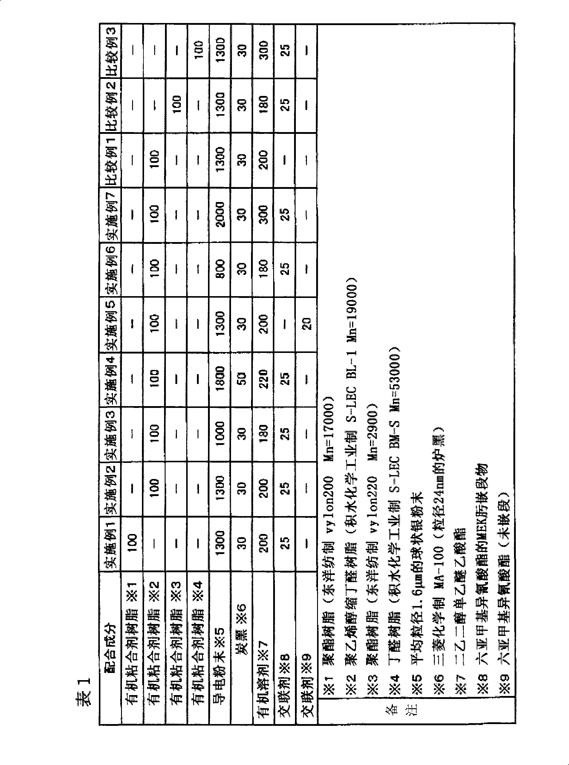
[0064] Each component was blended in the blending ratio shown in Table 1, and kneaded by a three-roll mill to obtain a conductive paste.
[0065]
[0066] Various characteristics of each conductive paste thus obtained were evaluated. The evaluation method is as follows.
[0067] (1) Determination of specific resistance value
[0068] A pattern of 0.5 cm×10 cm was formed on a glass substrate, and after heat treatment at 130° C. for 30 minutes, the resistance value was measured with a Milliohm HiTester, and the specific resistance value was calculated based on the sheet resistance and film thickness.
[0069] (2) Evaluation method of solvent resistance
[0070] After coating on a glass substrate with a 10 μm applicator and heat-treating at 130° C. for 30 minutes, rubbing solvent resistance was evaluated with acetone-impregnated waste cloth. The evaluation criteria are as follows.
[0071] ○: Almost no change
[0072] △: The coating film is slightly dissolved
[0073] ×:...
Embodiment 8~13 and comparative example 4~5
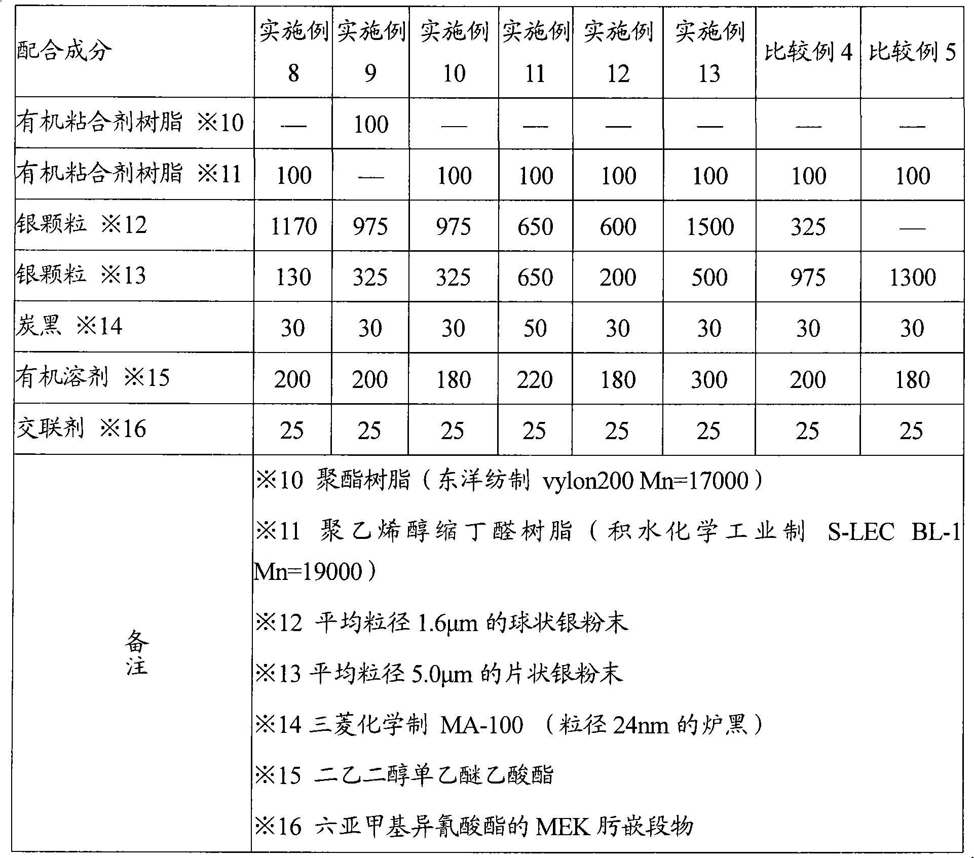
[0094] Each component was blended in the blending ratio shown in Table 3, and kneaded by a three-roll mill to obtain a conductive paste.
[0095] table 3
[0096]
[0097] Various characteristics of each conductive paste thus obtained were evaluated. The evaluation method is as described above.
[0098] These results are shown in Table 4.
[0099] Table 4
[0100]
[0101] From the results shown in Table 4, it can be seen that the conductive paste of the present invention can easily obtain a conductive pattern that has both conductivity and printability of thin lines. The visibility of the film was excellent.
PUM
| Property | Measurement | Unit |
|---|---|---|
| particle size | aaaaa | aaaaa |
| particle size | aaaaa | aaaaa |
| particle size | aaaaa | aaaaa |
Abstract
Description
Claims
Application Information
 - R&D Engineer
- R&D Manager
- IP Professional
- Industry Leading Data Capabilities
- Powerful AI technology
- Patent DNA Extraction
Browse by: Latest US Patents, China's latest patents, Technical Efficacy Thesaurus, Application Domain, Technology Topic, Popular Technical Reports.
© 2024 PatSnap. All rights reserved.Legal|Privacy policy|Modern Slavery Act Transparency Statement|Sitemap|About US| Contact US: help@patsnap.com


