Solid state image sensing device

A sensor device and solid-state image technology, applied in the field of solid-state image sensor devices, can solve problems such as deviation from the center position of the microlens and image sensor quality deterioration, and achieve the effect of eliminating sensitivity differences and improving quality

Active Publication Date: 2008-12-03
SOCIONEXT INC
View PDF3 Cites 5 Cited by
  • Summary
  • Abstract
  • Description
  • Claims
  • Application Information

AI Technical Summary

Problems solved by technology

[0008] For example, if figure 2 In the circuit shown, three transistors are arranged between the layout area of ​​PD2 and the layout area of ​​PD3, and there is a problem that since these three layout areas are connected laterally (that is, in the horizontal direction), due to the Periodic stripes (stripes) appear on the screen due to the difference in sensitivity
[0011] However, it cannot be solved that in an image sensor using shared pixels (in which the intervals between microlenses are not completely uniform), the center position of the photodiode as a light receiving unit (the intervals are almost uniform) deviates from the center of the microlenses. position and as the quality of the output of the image sensor deteriorates

Method used


Image

  • Solid state image sensing device
  • Solid state image sensing device
  • Solid state image sensing device

Examples


Embodiment Construction

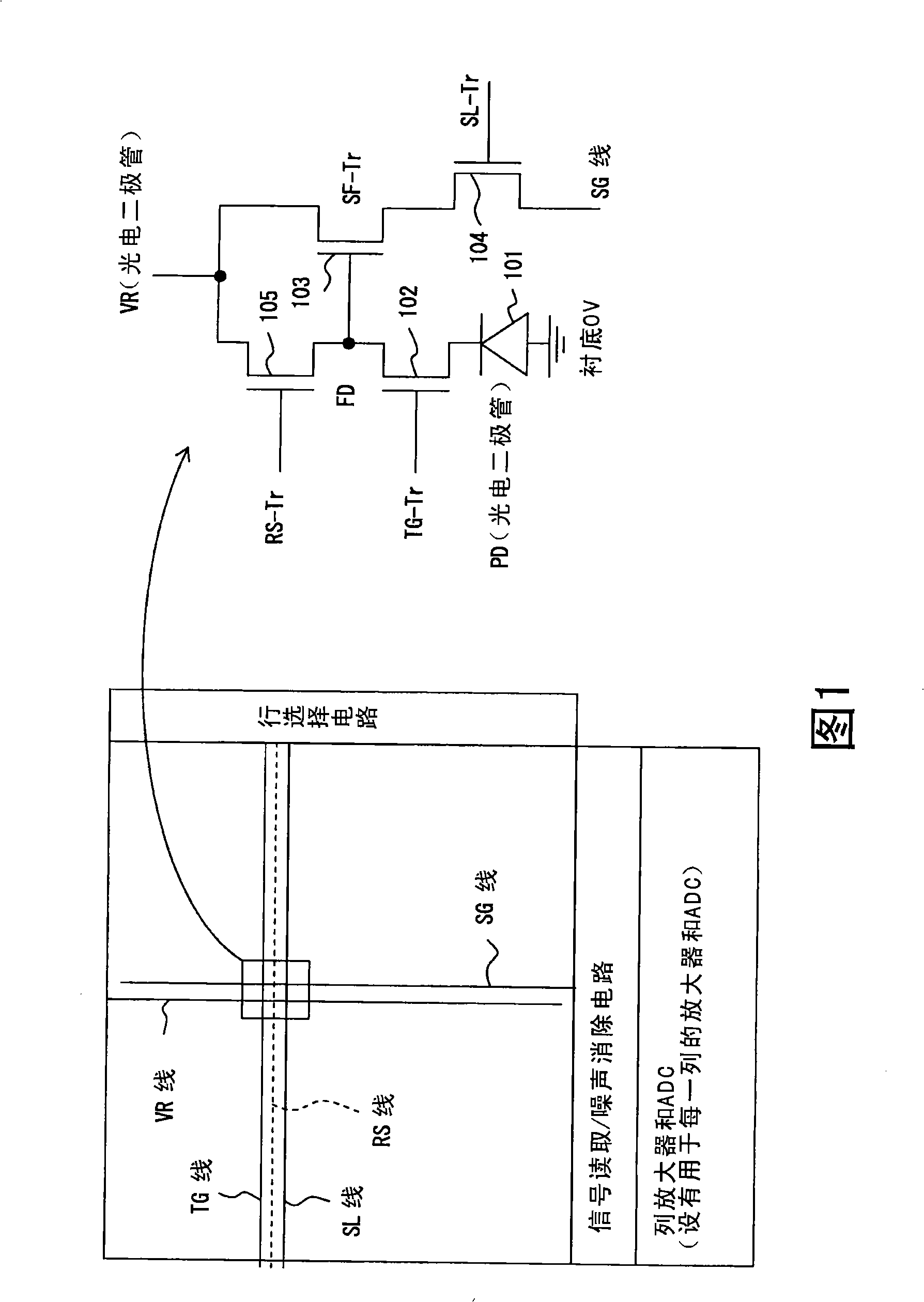
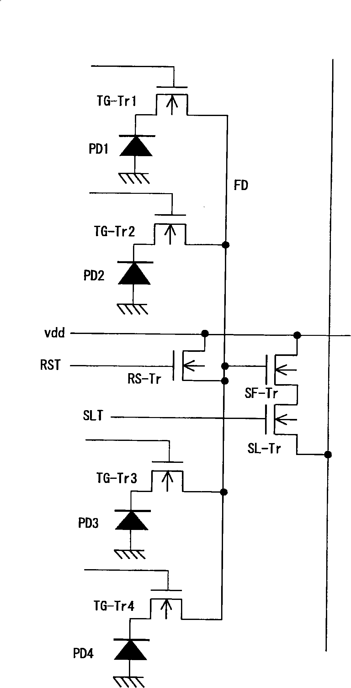
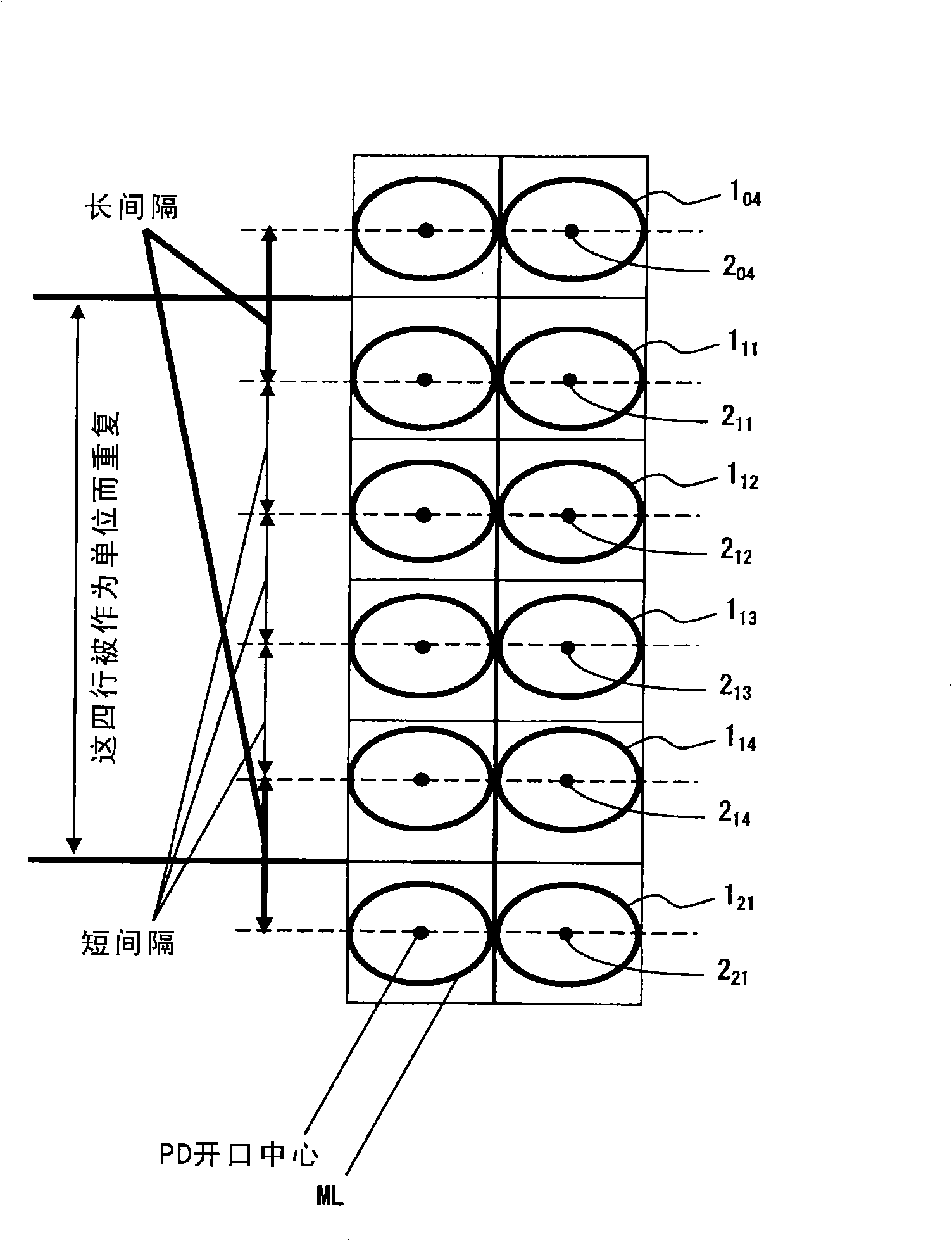
[0043] image 3 The arrangement method of the microlenses in the solid-state image sensing device of this preferred embodiment is explained theoretically. In the first half of the description of the present invention, the aim is to describe a shared type pixel in which a transistor for reading pixel data etc. The device—the central position of the microlens set in relation to each other) matches and arranges the photodiode in each pixel.

[0044] image 3 is a theoretical example. In this example, on a pixel plane where a plurality of pixels are arranged in columns and rows, photodiodes and microlenses are arranged in such a manner that periodically Change each center-to-center pitch of photodiodes and microlenses.

[0045] exist image 3 , four microlenses in each row direction 1 11 ~1 14 The microlens in corresponds to the four transistors sharing the pixel, and the centers of these four microlenses (2 11 ~2 14 ) The mutual interval between them is relatively short,...


PUM


Abstract

A solid state image sensing device in which many pixels are disposed in a matrix on a two-dimensional plane comprises a plurality of light receiving devices disposed in such a way that a center interval may periodically change in a column direction and / or a row direction, and a plurality of micro-lenses, for collecting an incident light of each light receiving device, wherein a center interval periodically changes in accordance with the periodic change of the center interval of the light receiving device.

Description

technical field [0001] The present invention relates to a solid-state image sensing device such as a CMOS image sensor on which a plurality of pixels are arranged in a matrix, and more particularly to a solid-state image sensing device using shared type pixels in which , a plurality of pixels share a part of transistors and the like for pixel data reading. Background technique [0002] Video cameras or digital still cameras use CCD or CMOS solid-state image sensing devices. In such a solid-state image sensing device, a plurality of pixels each having, for example, photodiodes as light receiving units are arranged in a matrix, and incident light entering each pixel is converted into electrons by the photodiodes to generate charge signals. The generated charge signal is output to the outside via the signal line. [0003] FIG. 1 shows pixels arranged in such a matrix and a related art read circuit for reading pixel data. FIG. 1 shows an example of a CMOS image sensor, which ...

Claims


Application Information

Patent Timeline
Patent Type & Authority Applications(China)
IPC IPC(8): H01L27/146H01L27/14H04N5/335H04N5/365H04N5/369H04N5/374H04N5/3745
CPCH01L27/14603H01L27/14621H01L27/14643H01L27/14627H01L27/14641H04N25/48
Inventor 井上忠夫大工博
Owner SOCIONEXT INC
Why Eureka
Try Eureka