Photoelectric conversion electrode, manufacturing method of the same, and dye-sensitized solar cell
A technology for photoelectric conversion electrodes and manufacturing methods, applied in capacitor electrodes, photovoltaic power generation, electrolytic capacitors, etc., can solve the problems of insufficient photoelectric conversion efficiency of photoelectric conversion elements, lack of tetrabromofluorescein co-adsorption pigment sensitization, etc., to achieve Improvement of production efficiency and economic benefits, high photoelectric conversion efficiency, and the effect of expanding the selection width
- Summary
- Abstract
- Description
- Claims
- Application Information
AI Technical Summary
Problems solved by technology
Method used
Image
Examples
no. 1 approach
[0040] figure 1 It is a schematic cross-sectional view schematically showing one embodiment of the photoelectric conversion electrode of the present invention. The photoelectric conversion electrode 11 is an electrode in which a porous metal oxide layer 14 including zinc oxide as a metal oxide and a sensitizing dye (pigment) is laminated on a substrate 12 having a conductive surface 12a.
[0041] The substrate 12 is not particularly limited as long as it can at least support the metal oxide layer 14, its type, size and shape. Plastic substrates such as ethylene glycol formate, polyethylene, polypropylene, and polystyrene, metal substrates or alloy substrates, ceramic substrates, or laminates thereof, and the like. Furthermore, the substrate 12 preferably has light transmittance, and more preferably has excellent light transmittance in the visible light region. Further, it is preferable that the base body 12 has bendability, and in this case, various forms of structures resul...
no. 2 approach
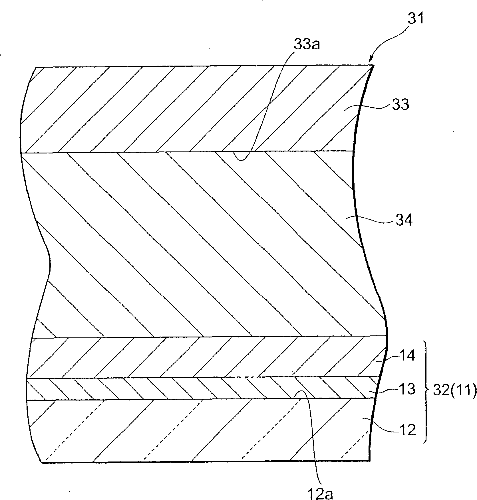
[0076] image 3 It is a schematic cross-sectional view schematically showing one embodiment of the dye-sensitized solar cell of the present invention. The dye-sensitized solar cell 31 has: the photoelectric conversion electrode 11 described in the above-mentioned first embodiment as the photoelectric conversion electrode 32; the counter electrode 33 arranged opposite thereto; 33 between charge transport layers 34 .
[0077] The conductive surface 33 a of the counter electrode 33 is arranged to face the metal oxide layer 14 . Moreover, as the counter electrode 33, a well-known counter electrode can be suitably used. For example, it can be an electrode having a conductive film on a transparent substrate like the substrate 12 having the conductive surface 12a of the photoelectric conversion electrode 11 described above, or an electrode on a transparent substrate. Electrodes of metal, carbon, conductive resin and other films are further formed on the conductive film.
[0078] A...
Embodiment 1
[0083] First, SnO doped with fluorine is used as the substrate 2 A transparent glass substrate with a transparent conductive film (trade name A110U80, manufactured by Asahi Glass Fabritech Co., Ltd.) was attached to one end of the transparent conductive film with a wire and connected to the working electrode of the stabilized power supply. Next, a masking tape having an opening of 40 mm×40 mm was covered on the surface of the transparent conductive film and the wire connection portion, and only the transparent conductive film was exposed at the opening, thereby producing a cover film portion.
[0084] Furthermore, a wire was connected to a zinc plate as a counter electrode, and an Ag / AgCl electrode as a reference electrode was connected to a reference point (reference). Thereafter, in a container made of polypropylene, the cover film portion of the transparent conductive film of the transparent glass substrate was arranged to face the counter electrode, and the reference elect...
PUM
| Property | Measurement | Unit |
|---|---|---|
| specific surface area | aaaaa | aaaaa |
| specific surface area | aaaaa | aaaaa |
| specific surface area | aaaaa | aaaaa |
Abstract
Description
Claims
Application Information
 - Generate Ideas
- Intellectual Property
- Life Sciences
- Materials
- Tech Scout
- Unparalleled Data Quality
- Higher Quality Content
- 60% Fewer Hallucinations
Browse by: Latest US Patents, China's latest patents, Technical Efficacy Thesaurus, Application Domain, Technology Topic, Popular Technical Reports.
© 2025 PatSnap. All rights reserved.Legal|Privacy policy|Modern Slavery Act Transparency Statement|Sitemap|About US| Contact US: help@patsnap.com


