Semiconductor device
一种半导体、双极晶体管的技术,应用在半导体器件、测量装置、电路装置等方向,能够解决不能充分增大感应比、过电流保护机能变大、偏差变大等问题,达到降低电流值的偏差、设置自由度增大、电连接的构造容易的效果
- Summary
- Abstract
- Description
- Claims
- Application Information
AI Technical Summary
Problems solved by technology
Method used
Image

Examples
Embodiment Construction
[0054] Hereinafter, a semiconductor device according to an embodiment of the present invention will be described with reference to the drawings.
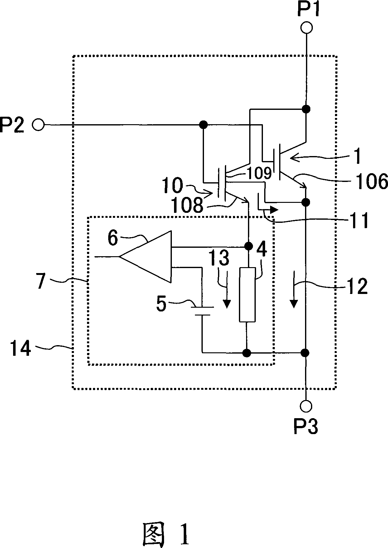
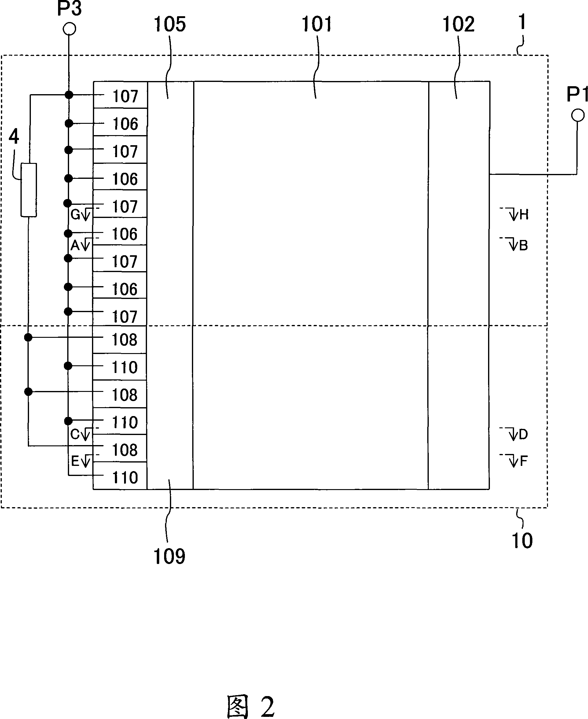
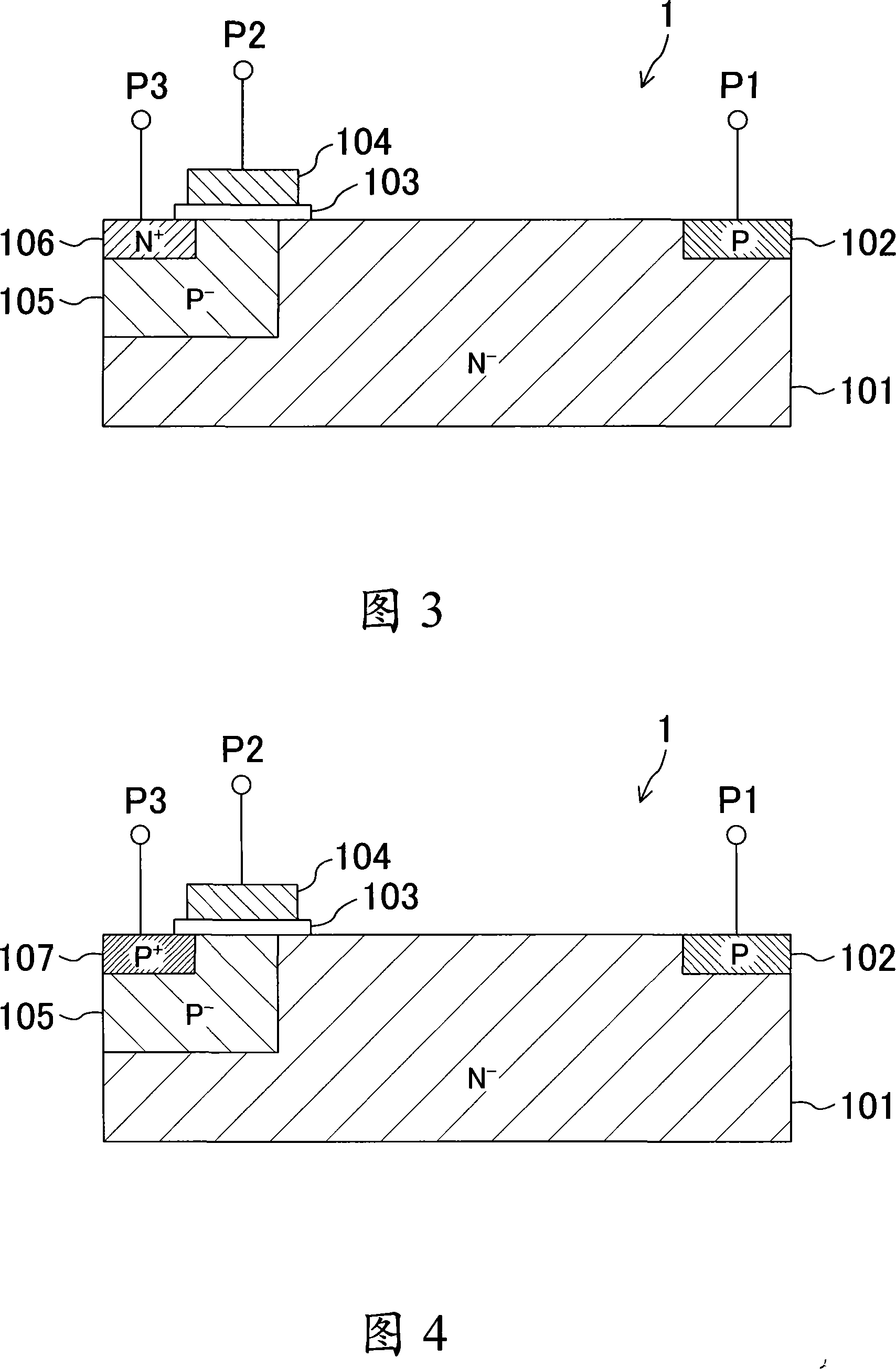
[0055] FIG. 1 is a schematic circuit configuration diagram showing a semiconductor device according to this embodiment, specifically, a semiconductor device having an overcurrent protection function for a horizontal insulated gate bipolar transistor.
[0056] A semiconductor device 14 shown in FIG. 1 has a horizontal IGBT 1 having a main switching element that can be controlled by a gate voltage, and a horizontal IGBT 10 for current detection is connected in parallel to the horizontal IGBT 1. connect. The respective collector regions and gate electrodes of the horizontal insulated gate bipolar transistor 1 and the current detection horizontal insulated gate bipolar transistor 10 are electrically connected to the collector terminal P1 and the gate terminal P2 . The emitter region (emitter region 106 ) of the horizontal IGBT 1 is ele...
PUM
 Abstract
Description
Claims
Application Information
 - R&D
- Intellectual Property
- Life Sciences
- Materials
- Tech Scout
- Unparalleled Data Quality
- Higher Quality Content
- 60% Fewer Hallucinations
Browse by: Latest US Patents, China's latest patents, Technical Efficacy Thesaurus, Application Domain, Technology Topic, Popular Technical Reports.
© 2025 PatSnap. All rights reserved.Legal|Privacy policy|Modern Slavery Act Transparency Statement|Sitemap|About US| Contact US: help@patsnap.com