Semiconductor isolation structure and forming method thereof

An isolation structure and semiconductor technology, applied in the direction of semiconductor devices, semiconductor/solid-state device manufacturing, electric solid-state devices, etc., can solve the problem that the manufacturing process isolation structure and semiconductor substrate affect device performance, the transistor loses the switching current control function, and the power consumption of the transistor Problems such as penetration through the layers can achieve the effects of easy control of the injection process, avoiding complex forming processes, and good isolation performance

Inactive Publication Date: 2008-08-20
SEMICON MFG INT (SHANGHAI) CORP
View PDF1 Cites 0 Cited by
  • Summary
  • Abstract
  • Description
  • Claims
  • Application Information

AI Technical Summary

Problems solved by technology

[0006] The formation method of the above-mentioned shallow trench isolation structure is relatively complicated, and there is stress between the liner oxide layer and the semiconductor substrate and between the liner oxide layer and the silicon oxynitride layer, and this internal stress will form defects in the active region ( defect) or cracks (cracks)
[0007] With the further development of technology, it is necessary to increase the density of devices in integrated circuits by reducing the size of devices. However, as the size of devices is further reduced, the complexity of the manufacturing process and the stress on the isolation structure and the semiconductor substrate and the isolation structure Issues that increasingly affect the performance of the device
[0008] In addition, the semiconductor substrate of the above-mentioned shallow trench isolation structure is silicon. After forming a semiconductor device such as a transistor on the semiconductor substrate, the channel layer of the transistor is located on the surface of the silicon substrate. For semiconductor devices of 65nm and below , the channel length of the transistor is relatively short, the source and drain in the substrate are very close, it is easy to cause the depletion layer of the transistor to penetrate, and the leakage current flows from the semiconductor silicon substrate, causing the transistor to lose the control function of switching current

Method used


Image

  • Semiconductor isolation structure and forming method thereof
  • Semiconductor isolation structure and forming method thereof
  • Semiconductor isolation structure and forming method thereof

Examples


Embodiment Construction

[0027] The specific embodiments of the present invention will be described in detail below in conjunction with the accompanying drawings.

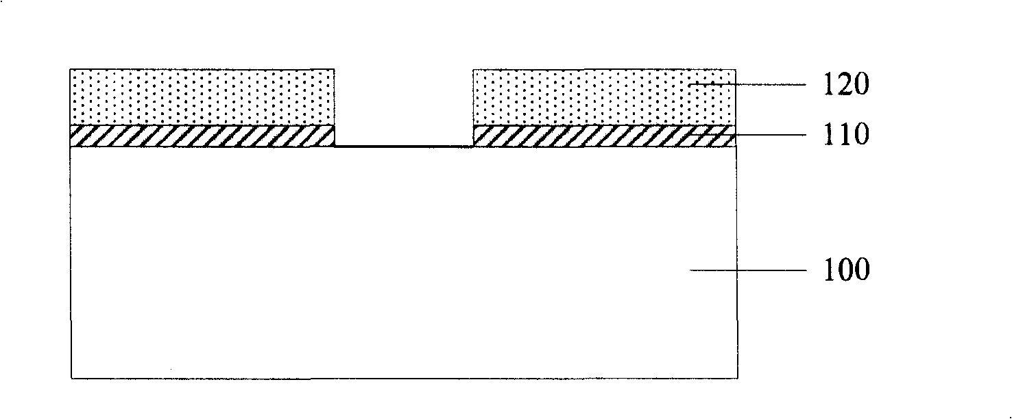
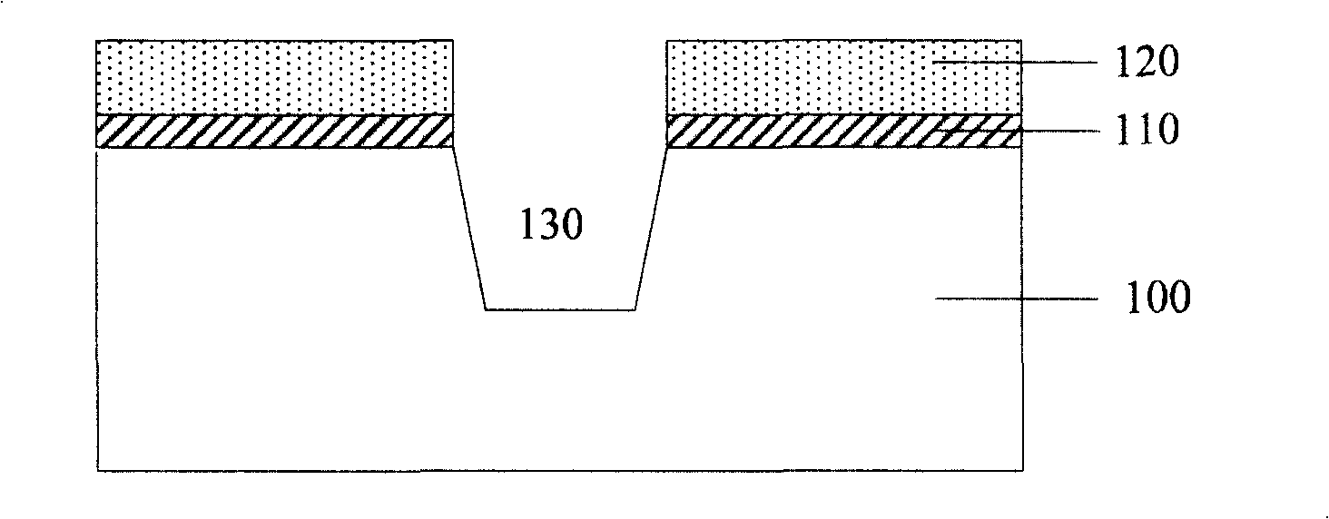
[0028] The manufacturing method of the semiconductor isolation structure of the present invention is to form a planarized isolation region between the active regions of the semiconductor device by using an oxygen ion implantation method on the semiconductor substrate with a sacrificial oxide layer formed on the surface, and the semiconductor substrate is Silicon on insulator, under the conditions of different ion implantation energies and ion doses, perform oxygen ion implantation one or more times, and then perform annealing treatment to form an isolation structure.

[0029] Reference attached Figure 7 Shown is a process flow chart of the method for forming the semiconductor isolation structure of the present invention. Such as Figure 7 As shown, the method for forming the isolation structure of the present invention includes: step S1...


PUM


Abstract

The invention is a method for forming a semiconductor isolation structure, comprising the steps of: providing a semiconductor substrate which is a silicon on insulated substrate; forming a sacrificial oxide layer on the semiconductor substrate; forming a mask on the sacrificial oxide layer, and patterning the mask to define an active region and a isolated region on the semiconductor substrate; implanting oxygen ions to the isolated region through the sacrificial oxide layer; removing the mask; annealing the semiconductor substrate to arrange the oxygen ions ions evenly, thus forming the isolation structure; and removing the sacrificial oxide layer. According to the invention, the process is simple, the complexity of current preparing process of a STI isolated structure is avoided, and the defect that stress exists between a lining oxide layer and a semiconductor substrate, and between a lining oxide layer and a silicon oxynitride layer is also overcome.

Description

technical field [0001] The invention relates to the technical field of semiconductor manufacturing, in particular to a method for forming a semiconductor isolation structure and the isolation structure. Background technique [0002] Semiconductor integrated circuits generally contain active regions and isolation regions between the active regions, which are formed prior to fabrication of the active devices. Methods for forming isolation regions in the prior art mainly include Local Oxygen Isolation (LOCOS) and Shallow Trench Isolation (STI). The LOCOS process is to deposit silicon oxide and silicon nitride layers on the surface of the wafer, and then etch the silicon nitride layer to form a trench, and grow an isolation oxide layer in the trench area. Due to the different thermal expansion properties between silicon nitride and silicon during the oxidation process, at the boundary between silicon nitride and silicon oxide, oxygen diffuses through silicon oxide to the bottom...

Claims


Application Information

Patent Timeline
Patent Type & Authority Applications(China)
IPC IPC(8): H01L21/76H01L27/12
Inventor 肖德元
Owner SEMICON MFG INT (SHANGHAI) CORP
Why Eureka
Try Eureka