Inner pin joint packaging
A technology of inner pins and pins, which is applied in the field of semiconductor packaging structures, can solve the problems of inability to complete eutectic bonding consistently, insufficient eutectic strength of thick legs, tin overflow of thin legs, etc.
- Summary
- Abstract
- Description
- Claims
- Application Information
AI Technical Summary
Problems solved by technology
Method used
Image
Examples
Embodiment Construction
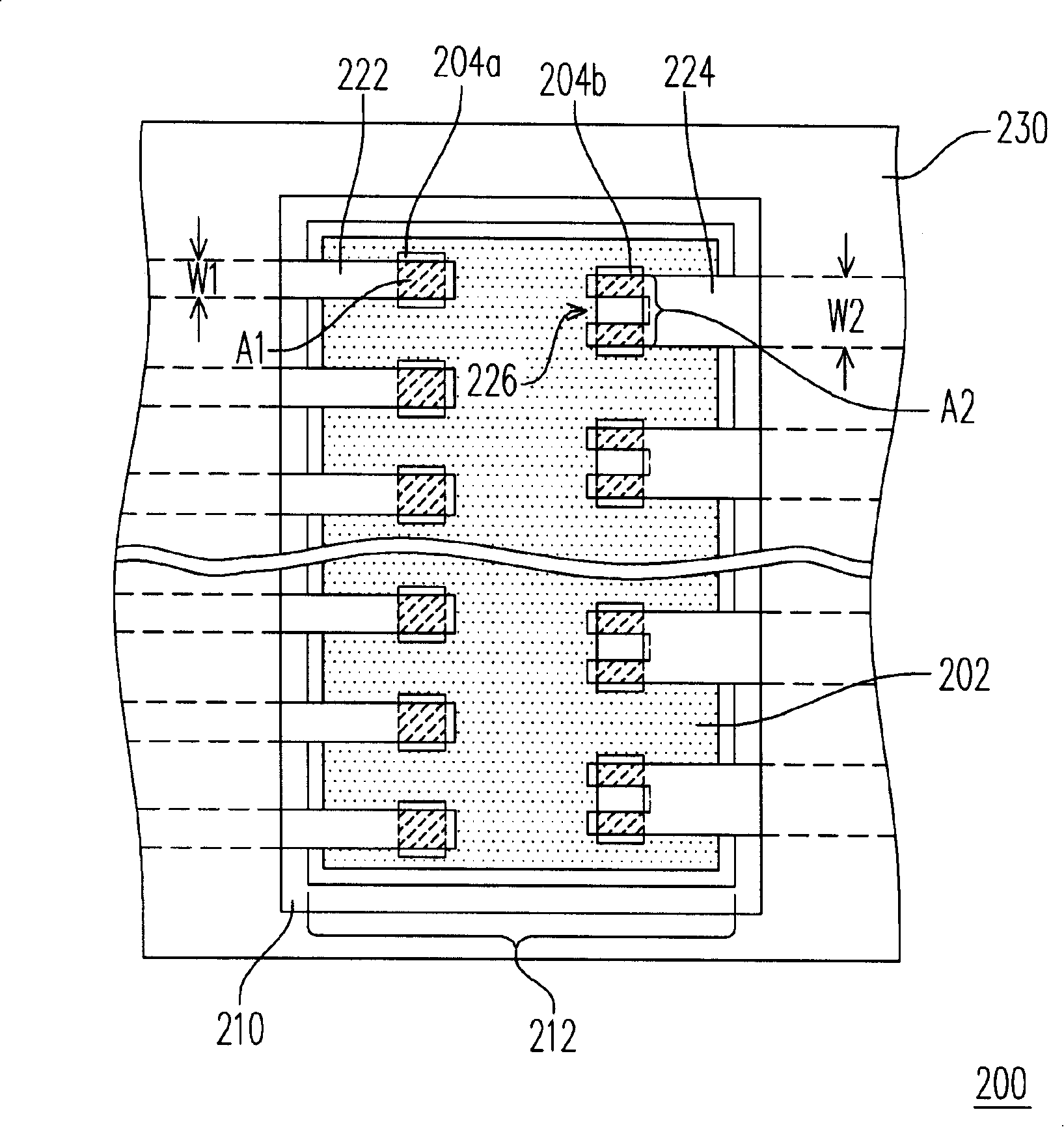
[0014] image 3 It is a top view of an embodiment of a pin-bonded chip package structure in the present invention. Please refer to image 3 , the internal pin bonding package 200 includes a chip 202 , a flexible board 210 , and pins 222 and 224 disposed on the flexible board 210 and electrically connected to the chip 202 . In this internal pin bonding package 200, the gold bumps or other solder bumps on the chip 202 are first completed, and the pins 222, 224 and the solder mask 230 on the flexible board 210 are completed, and then bonded by thermocompression or In the way of ultrasonic bonding, the bumps 204a, 204b on the chip 202 are electrically connected to the inner ends of the pins 222, 224 by gold-tin eutectic bonding. Although the present invention is described with a tape carrier package (TCP, tape carrier package) flexible board or a film-on-film (COF, chip on film) flexible board used in the tape automatic bonding process as a preferred example, those skilled in th...
PUM
 Abstract
Description
Claims
Application Information
 - R&D
- Intellectual Property
- Life Sciences
- Materials
- Tech Scout
- Unparalleled Data Quality
- Higher Quality Content
- 60% Fewer Hallucinations
Browse by: Latest US Patents, China's latest patents, Technical Efficacy Thesaurus, Application Domain, Technology Topic, Popular Technical Reports.
© 2025 PatSnap. All rights reserved.Legal|Privacy policy|Modern Slavery Act Transparency Statement|Sitemap|About US| Contact US: help@patsnap.com


