Connection device between packaging substrate and chip thereon

A technology of connecting device and packaging base, which is applied to printed circuits, printed circuit components, electrical components and other directions where non-printed electrical components are connected, can solve the problem of low yield of connecting leads, multiple waste products, and long connecting lead lengths. and other problems, to achieve the effect of low cost, avoiding excessive sagging and reducing length

Inactive Publication Date: 2008-07-02
SEMICON MFG INT (SHANGHAI) CORP
View PDF0 Cites 3 Cited by
  • Summary
  • Abstract
  • Description
  • Claims
  • Application Information

AI Technical Summary

Problems solved by technology

[0004] Chips are becoming more and more miniaturized. If cost and cycle are considered, the use of existing substrates for large wafers will result in longer lengths of connecting wires, especially when using such as figure 2 The configuration shown requires a longer connecting lead length in the diagonal direction
Excessive sag and "wiggle" when using longer connecting leads, and too low connecting lead yield resulting in too much scrap

Method used


Image

  • Connection device between packaging substrate and chip thereon
  • Connection device between packaging substrate and chip thereon
  • Connection device between packaging substrate and chip thereon

Examples


Embodiment Construction

[0021] Embodiments of the present invention will be described in detail below in conjunction with the accompanying drawings, wherein similar structures in the accompanying drawings use the same reference numerals.

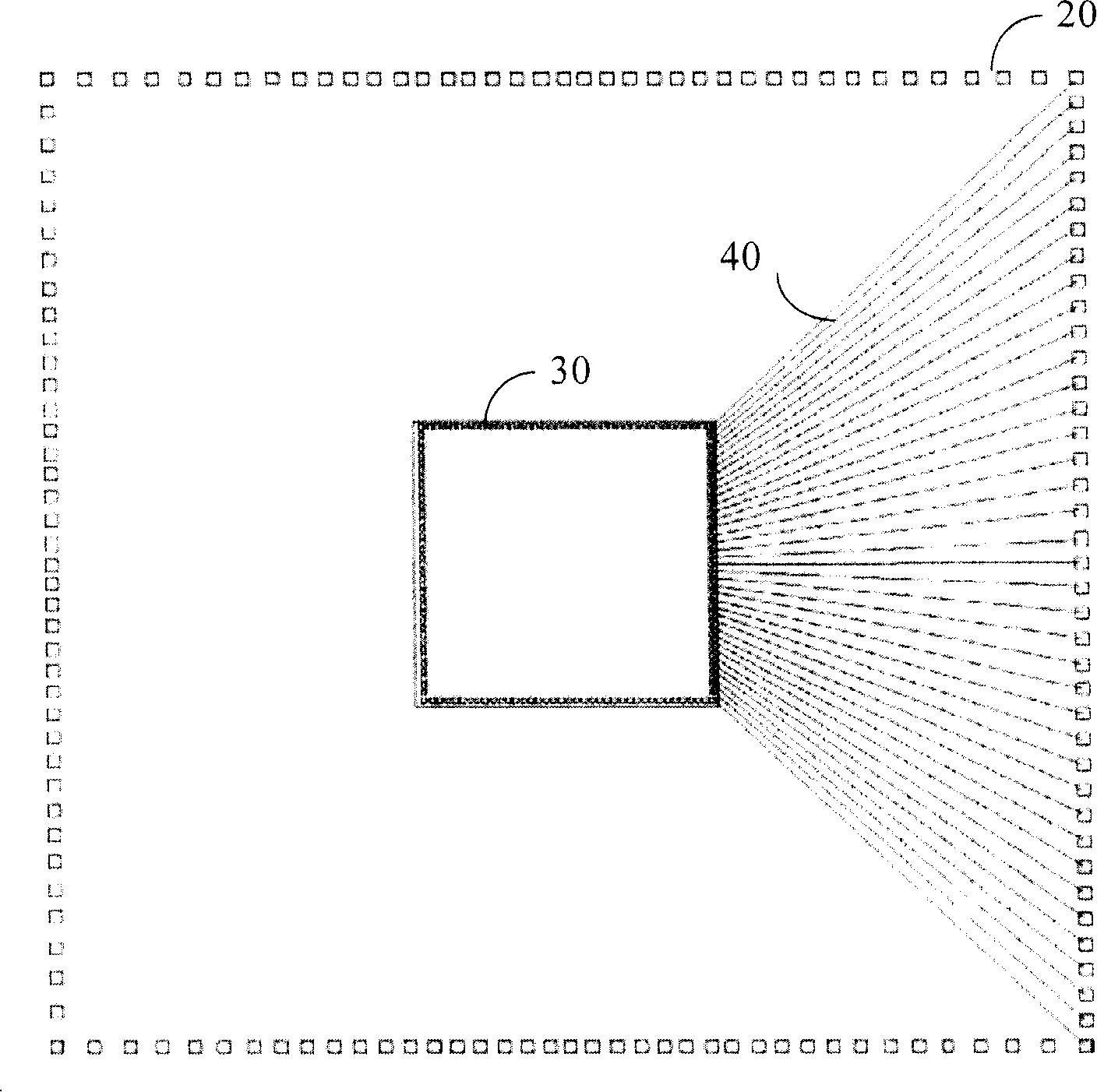
[0022] According to the present invention, there is provided a connection device between a packaging substrate and a chip thereon, comprising: a plurality of finger pad rings surrounding the chip on the packaging substrate, each finger pad ring including multiple and a plurality of connection leads for connecting the chip to the pad fingers of the innermost ring of pad fingers and for connecting pad fingers of adjacent pad finger rings.

[0023] Such as figure 1 As shown, the PCB includes a package substrate 10, a ring of solder fingers 20 and a chip 30 located in the center of the package substrate, and the ring of solder fingers 20 includes a plurality of solder fingers made of gold or other materials materials known in the art. The pins of the solder fingers a...


PUM


Abstract

The invention provides a device for connecting a packaging substrate with a chip on the packaging substrate, which comprises a plurality of figure-like solder sheet rings on the packaging substrate which enclose the chip; each figure-like solder sheet ring comprises a plurality of figure-like solder sheets; and a plurality of connection lead wires which are used for connecting the chip and the figure-like solder sheet of the innermost ring of the figure-like solder sheet ring and for connecting the figure-like solder sheet of the neighboring figure-like solder sheet ring. The invention also provides a printed circuit board with the connection device, By adopting the technical proposal of the invention, length of the connection lead wire can be effectively reduced under a condition of small-sized chip, thereby effectively avoiding generation of excessive droop and swing as well as increasing yield of the connection lead wire and reducing cost. In particular to non-amount-production application like engineering verification and reliability test, the invention has practical value. Under a condition of limited available substrate, product function and reliability can be verified and evaluated rapidly with low cost, which wins the time for the follow-up market operation and mass production.

Description

technical field [0001] The present invention generally relates to packaging substrates, and more particularly to connection devices between packaging substrates and chips thereon. Background technique [0002] In the semiconductor industry, product reliability testing and chip characteristics such as electrostatic discharge (ESD) and gate lock-up (Latch-up) are becoming more and more important for technical quality monitoring. Among them, chip assembly is the product reliability testing and It is a necessary step before other engineering tests, but the design and manufacture of many chip assemblies including related assembly materials (such as packaging substrates) requires a long period (generally two to three months). And more and more products with different packaging types require product reliability testing, such as ESD and Latch-up testing are necessary for product quality or IP release. Since the packages of various chips have different lead counts and lead definitio...

Claims


Application Information

Patent Timeline
Patent Type & Authority Applications(China)
IPC IPC(8): H05K1/02H01L23/498H01L23/488H05K1/18
CPCH01L2924/0002
Inventor 简维廷刘云海郭强覃碨珺马瑾怡张荣哲
Owner SEMICON MFG INT (SHANGHAI) CORP
Why Eureka
Try Eureka