
Control circuit and method for controlling a plurality of a plurality of EEPROM operation modes of MCU series products

A technology for controlling circuits and working modes, applied in electrical digital data processing, instruments, etc., can solve problems that cannot meet product design flexibility, reliability, testability, etc., to optimize system architecture, improve system functions, and expand applications Effect

Active Publication Date: 2008-06-25
SHANGHAI HUAHONG GRACE SEMICON MFG CORP
View PDF0 Cites 7 Cited by
  • Summary
  • Abstract
  • Description
  • Claims
  • Application Information

AI Technical Summary

Problems solved by technology

This method is greatly limited in MCU chips with built-in multiple memories (programs and data), and cannot meet the requirements of product design flexibility, reliability, and testability.

Method used


Image

  • Control circuit and method for controlling a plurality of a plurality of EEPROM operation modes of MCU series products
  • Control circuit and method for controlling a plurality of a plurality of EEPROM operation modes of MCU series products
  • Control circuit and method for controlling a plurality of a plurality of EEPROM operation modes of MCU series products

Examples


Embodiment Construction

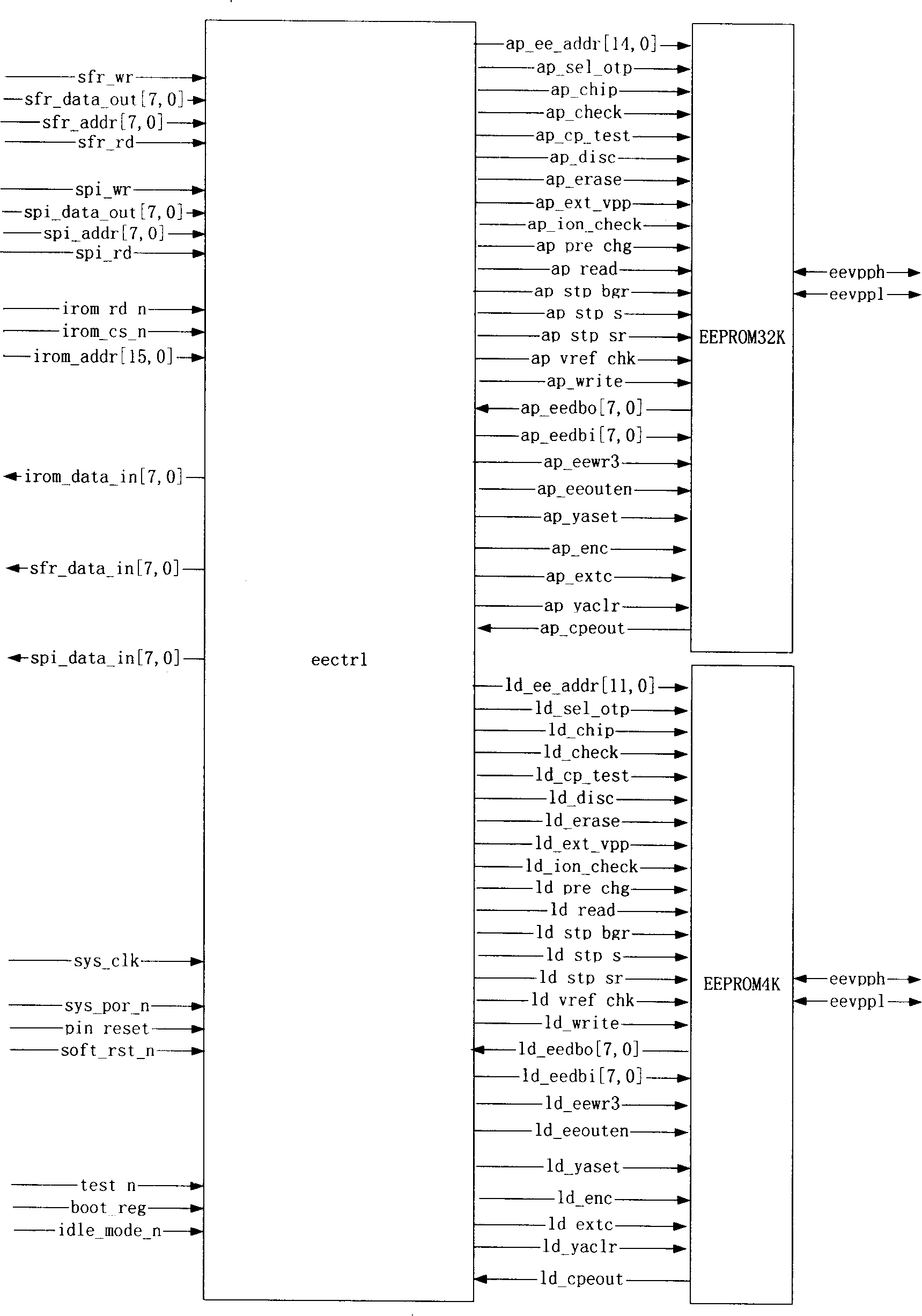
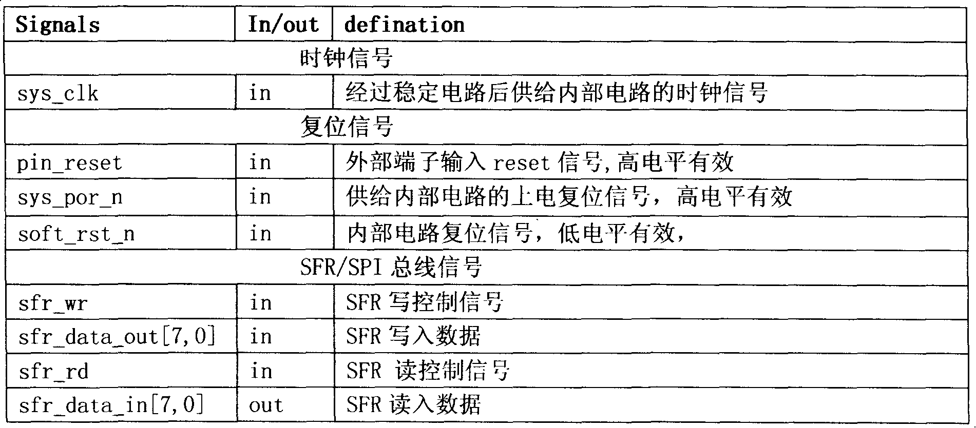
[0010] Such as figure 1 As shown, the EEPROM control circuit of the present invention uses verilog to carry out circuit design and simulation and is verified by the FPGA system. A group of special registers are arranged in the control circuit. By setting different control words for the special registers, multiple access to an EEPROM memory. The control circuit also includes three interface buses, namely SFR (special register) interface bus, MCU (micro controller unit) instruction reading interface bus and serial programming (SPI) interface bus. Wherein the MCU is connected to the control circuit through the SFR interface bus and the MCU command reading interface bus, and the serial programming module is connected to the control circuit through the SPI interface bus. Wherein, the SPI interface bus and the SFR interface bus jointly control the special registers in the control circuit, so that the serial programming module or MCU can read, write, address, Data input and data ou...


PUM


Abstract

The present invention discloses a control circuit and method for controlling a plurality of EEPROM working modes in MCU products, which can control a plurality of EEPROMs in MCU products to work under different modes of program access, serial writing, memory test and system programming on the basis of adding no extra circuit consumption. The application of the control circuit is realized through the following methods that: when the EEPROMs need to work under a serial writing mode, the connection of the access channels between data buses of the EEPROMs and a SPI interface bus is opened; when the EEPROMs need to work under an ISP mode, the access channels between the corresponding data buses of the loading EEPROMs and a MCU instruction reading interface bus are opened, and the access channels between the corresponding data buses of the application EEPROMs and a SFR interface bus are opened; when the EEPROMs need to work under a test mode, the access channels between the data buses of all the EEPROMs and the SFR interface bus are opened; when the EEPROMs need to work under a normal application mode, the access channels between the data buses of all the EEPROMs and the SFR interface bus are opened.

Description

technical field [0001] The invention relates to a control circuit for controlling multiple EEPROM working modes in MCU products. The invention also relates to a method for using the control circuit to control multiple EEPROM working modes in MCU products. Background technique [0002] In MCU products, the memory is a very basic module unit, and the most common application of EEPROM is as a program memory. The usual design method is that the MCU accesses the EEPROM through the program bus, and then designs a part of the programming control circuit to realize the EEPROM. For programming, the test uses BIST (built-in self-test) method to test the memory. This method is greatly limited in MCU chips with built-in multiple memories (programs and data), and cannot meet the requirements of product design flexibility, reliability, and testability. Contents of the invention [0003] The technical problem to be solved by the present invention is to provide a control circuit for con...

Claims


Application Information

Patent Timeline
Patent Type & Authority Applications(China)
IPC IPC(8): G06F13/40G06F13/16
Inventor 刘浩
Owner SHANGHAI HUAHONG GRACE SEMICON MFG CORP
Learn More