
Image sensing device and manufacturing method thereof

An image sensing and manufacturing method technology, applied in radiation control devices, semiconductor/solid-state device manufacturing, electrical components, etc., can solve the problems of decreased photosensitive effect of photodiode 74, increased leakage current noise, surface defects, etc. Effects and sensitivity, improved resolution, shorter optical path effects

Active Publication Date: 2008-02-27
UNITED MICROELECTRONICS CORP
View PDF2 Cites 18 Cited by
  • Summary
  • Abstract
  • Description
  • Claims
  • Application Information

AI Technical Summary

Problems solved by technology

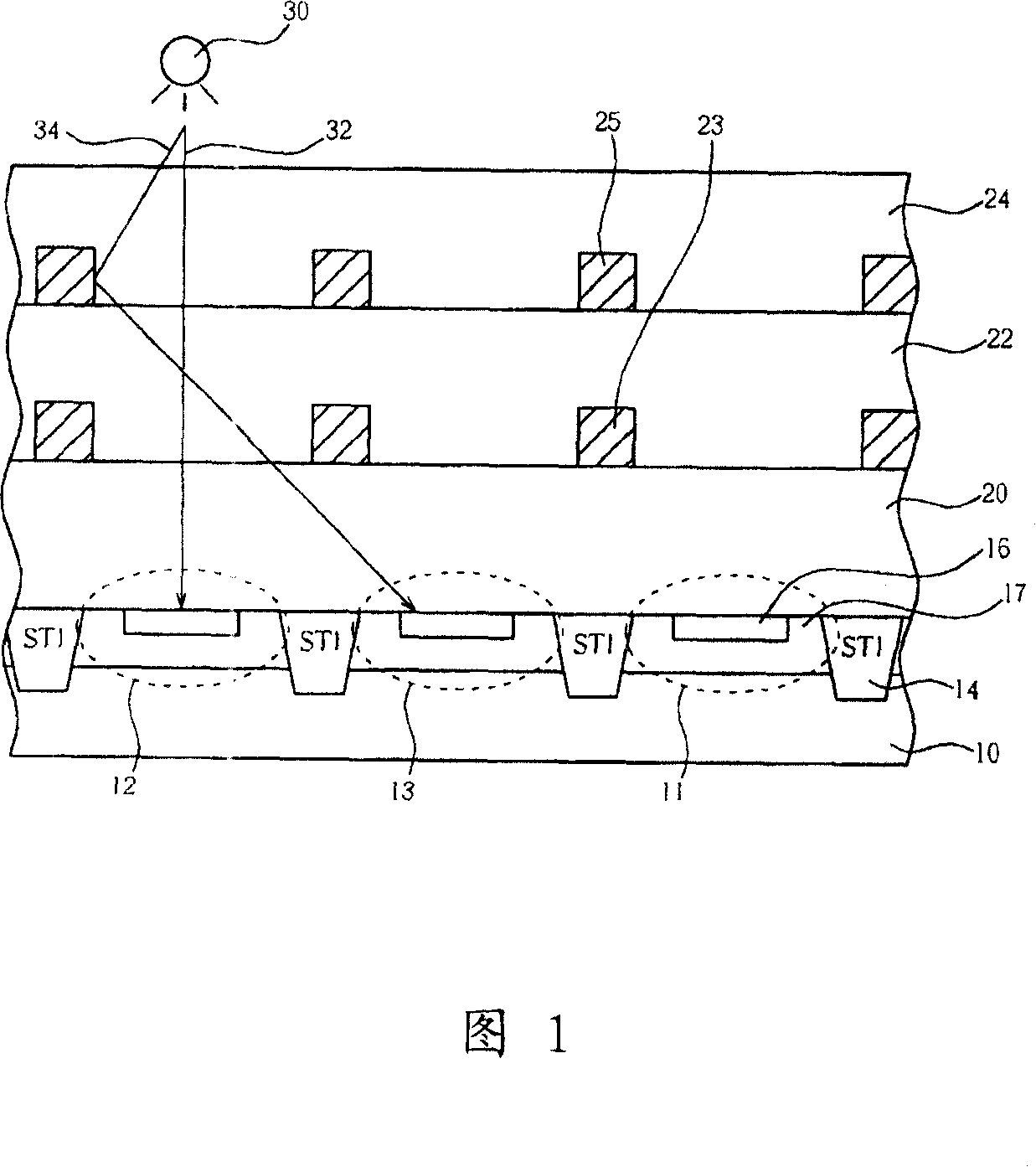
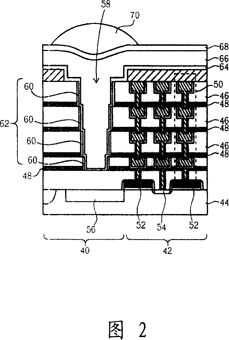
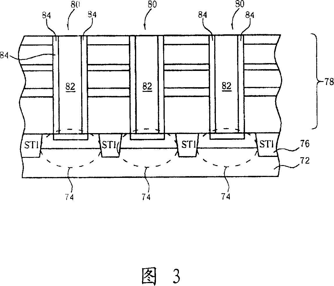
However, since the disclosed optical channel 80 is directly connected to the photodiode 74, in an actual process, when the optical channel 80 is etched, the surface of the photosensitive area of ​​the photodiode 74 is very vulnerable to plasma damage ( Plasma damage) and the pollution of impurity residues will produce a large number of surface defects, increase the leakage current and cause noise, so that the photosensitive effect of the photodiode 74 will decrease. In severe cases, it will even cause damage to the photodiode 74 and lose its function

Method used


Image

  • Image sensing device and manufacturing method thereof
  • Image sensing device and manufacturing method thereof
  • Image sensing device and manufacturing method thereof

Examples


Embodiment Construction

[0049] In order to highlight the advantages and features of the present invention, a preferred embodiment of the present invention is listed below, and is described in detail in conjunction with the drawings as follows:

[0050] 4 to 10 are process schematic diagrams of the image sensing device of the present invention. First please refer to FIG. 4 , a substrate 100 is provided, on which at least one optical element 106, at least one insulator 105 isolating the optical element 106, at least one interlevel dielectric layer (interlevel dielectric layer, ILD) 112, multilayer Intermetal dielectric layers (intermetal dielectric layer, IMD) 114 , 116 , 118 and a plurality of metal wires 107 , 108 , 109 . In this preferred embodiment, the substrate 100 is a semiconductor substrate, but not limited to a silicon wafer (wafer) or a silicon-on-insulator (SOI) substrate; the optical element 106 can be a photodiode (photodiode), used for Receive external light and sense the intensity of l...


PUM


Abstract

An image-sensing device includes a substrate, at least one optic component, at least one dielectric layer and at least a waveguide set above the optic component. Sidewall of the waveguide is set with a optic-shielding layer, and the waveguide is embedded with a filling layer. Therefore, the device can effectively shorten optic path, focus light, and avoid bridging phenomenon between different optic paths to improve sensitivity of the image-sensing device.

Description

technical field [0001] The invention relates to an image sensing device with a waveguide and a manufacturing method thereof. Background technique [0002] Complementary metal-oxide-semiconductor transistor image sensor (CMOS image sensor, CIS) is a common image sensing device today, and because CIS can be integrated into traditional semiconductor manufacturing, it has low manufacturing cost and low device size. Smaller and higher integration (integration) advantages. In addition, CIS also has the advantages of low operating voltage, low power consumption, high quantum efficiency, low noise (read-out noise), and random access according to needs, so it has been widely used in personal computer cameras ( PC camera) and digital camera (digital camera) and other electronic products. [0003] A typical CIS structure can be divided into a photo-sensing area and a peripheral circuit area according to its function. The photo-sensing area is usually provided with a plurality of phot...

Claims


Application Information

Patent Timeline
IPC IPC(8): H01L27/146H01L21/82G02B6/12G02B6/13
Inventor 柯登渊彭念祖陈坤助
Owner UNITED MICROELECTRONICS CORP
Learn More