Container conversion device for semi-conductor packaging element

A conversion device, semiconductor technology, applied in furnace components, conveyor objects, transportation and packaging, etc., can solve the problems of easy bumping of semiconductor components, large labor demand, slow speed, etc.

Inactive Publication Date: 2008-01-30
KING YUAN ELECTRONICS
View PDF0 Cites 5 Cited by
  • Summary
  • Abstract
  • Description
  • Claims
  • Application Information

AI Technical Summary

Problems solved by technology

Semiconductor packaged components are usually transported on trays after packaging. However, tube handlers are often used for testing during testing operations. Therefore, semiconductor packaged components must first be converted from trays to tubes. (tube) to facilitate the test operation; in addition, some directly use pallets for testing, but need to use tubes for shipment when shipping
In traditional testing operations, when semiconductor components must be transferred from pallet containers to tubes, if the conversion is done manually, it not only requires a lot of manpower and is slow, but also easily damages the semiconductor components

Method used


Image

  • Container conversion device for semi-conductor packaging element
  • Container conversion device for semi-conductor packaging element
  • Container conversion device for semi-conductor packaging element

Examples


Embodiment Construction

[0049] Embodiments of the present invention are described in detail as follows, however, the present invention can be widely implemented in other embodiments besides the detailed description. That is to say, the scope of the present invention is not limited by the proposed embodiments, but should be based on the patent scope of the present invention.

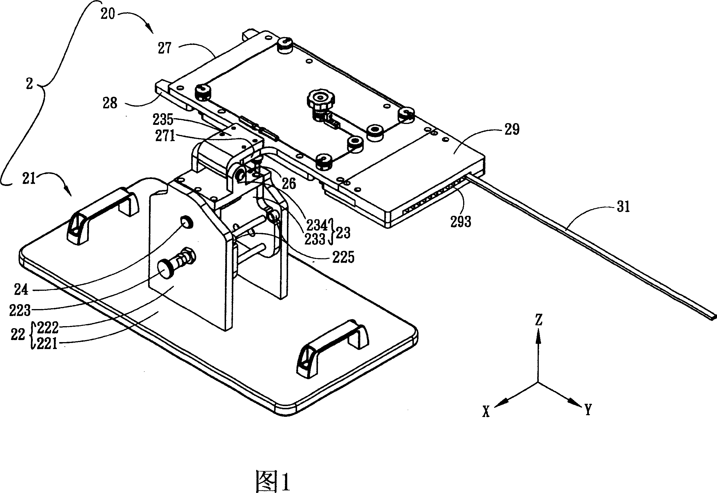
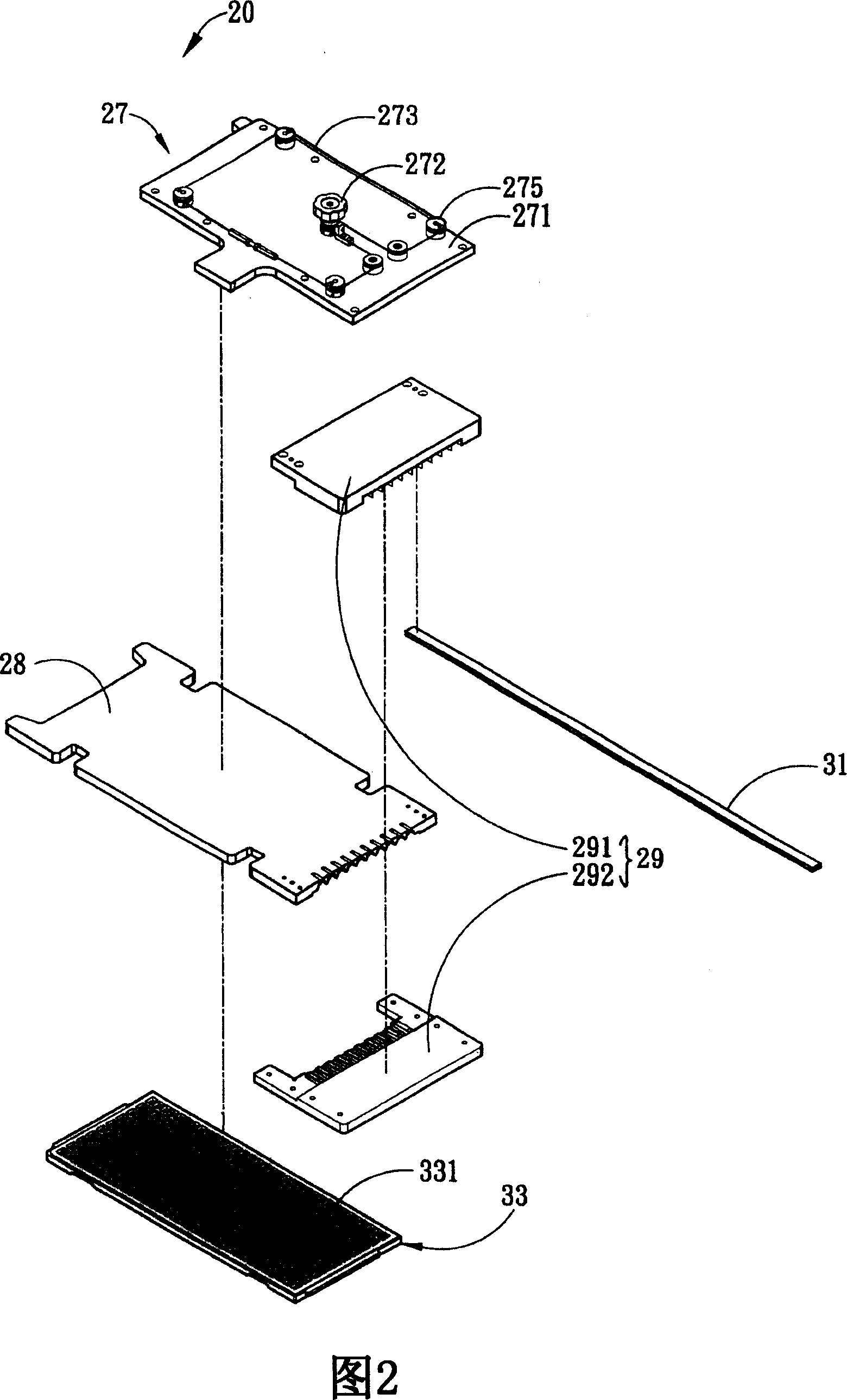
[0050] The perspective view of FIG. 1 shows a container conversion device 2 for semiconductor packaging components according to an embodiment of the present invention, which mainly includes a pallet clamping mechanism module 20 and a biaxial rotating mechanism module 21 . Wherein, the exploded view of the constituent elements of the clamping tray mechanism module 20 is shown in FIG. There are a plurality of accommodating grooves 331 respectively used for accommodating a semiconductor component (not shown in the drawing). The tray clamping mechanism module 20 mainly includes a slideway base plate 28 , a tray clamp 27 and an intu...


PUM


Abstract

A container conversion device of a semiconductor mounting element includes a clamp tray mechanism module and a dual-shaft rotary mechanism module. The clamp tray mechanism module includes a tray clamp, a slide way base plate and an insertion pipe mechanism. The surface of the slide way base plate is provided with a plurality of slide ways arranged on the lower surface of the tray clamp. The outlet of the slide way of the slide way base plate is provided with the insertion pipe mechanism; each material pipe insertion trough of the insertion pipe mechanism can be inserted by a material pipe. The clamp tray mechanism module is articulated with the dual-shaft rotary mechanism. When the clamp tray mechanism module at the horizontal position clamps the tray which is supported with a plurality of semiconductor mounting elements, by the rotation of 180 DEG of the second rotary shaft of the dual-shaft rotary mechanism module, each line of semiconductor mounting element on the tray is dropped into each slide way of the slide way base plate and slides into the material pipe of the insertion pipe mechanism along the slide way. The invention has the advantages of fast and easy replacement by adopting the modularization design, aiming at the semiconductor mounting elements of different types and dimensions.

Description

technical field [0001] The invention relates to a container switching device, in particular to a container switching device for semiconductor packaging components, which is used for quickly switching semiconductor packaging components placed in a tray to a tube. Background technique [0002] After the semiconductor wafer is designed and manufactured, the electrical function of the assembled product must be tested by a tester to ensure the normal function of the integrated circuit on the wafer. Semiconductor packaged components are usually transported on trays after packaging. However, tube handlers are often used for testing during testing operations. Therefore, semiconductor packaged components must first be converted from trays to tubes. (tube) to facilitate the test operation; in addition, some directly use pallets for testing, but need to use tubes for shipment when shipping. In traditional testing operations, when semiconductor components must be transferred from tray ...

Claims


Application Information

Patent Timeline
Patent Type & Authority Applications(China)
IPC IPC(8): B65G49/07B65G47/74H01L21/677
Inventor 林源记黎孟达
Owner KING YUAN ELECTRONICS
Why Eureka
Try Eureka