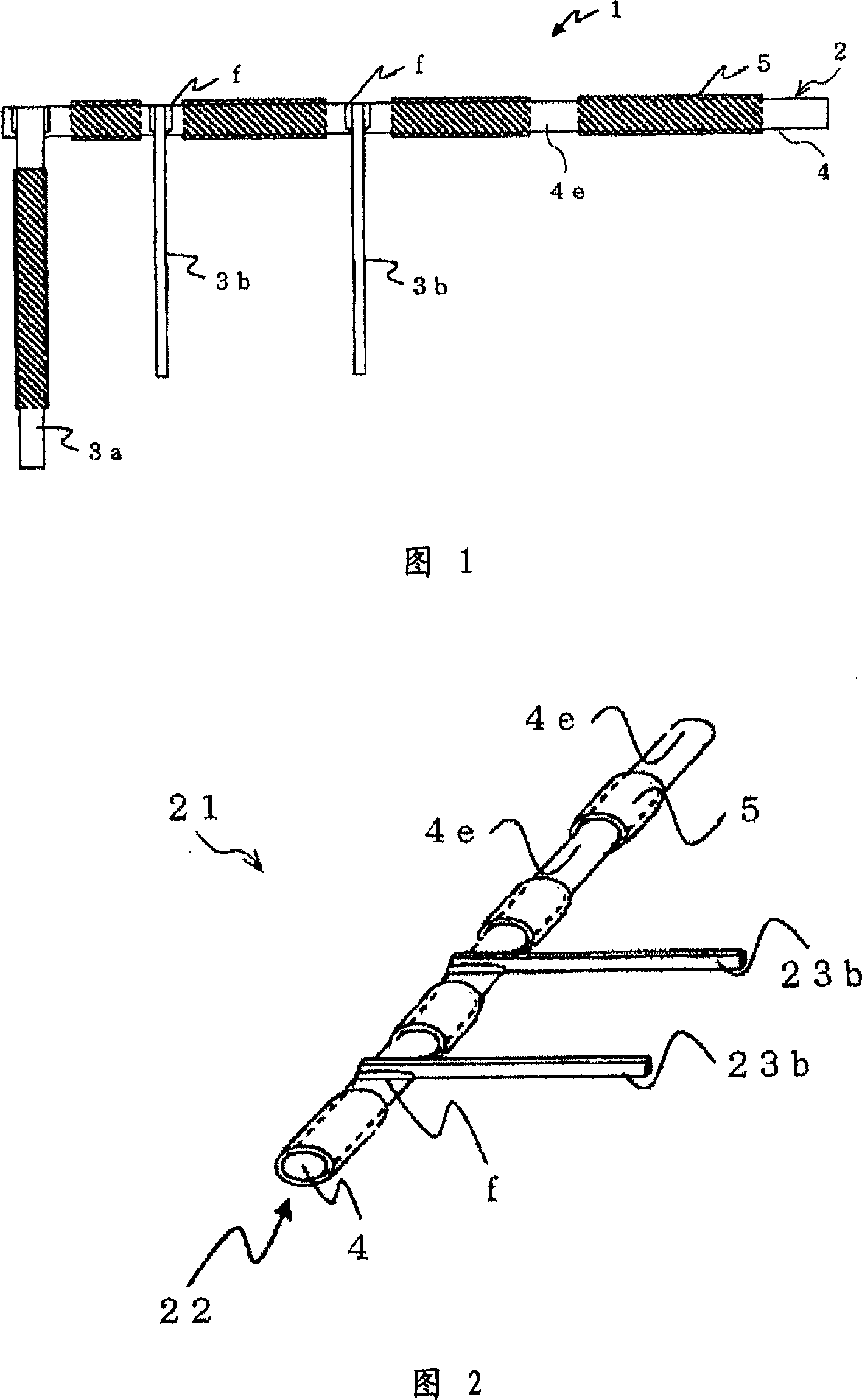
Connecting lead wire, method for fabricating same, and solar battery module using the connecting lead wire
A technology for solar cells and connecting leads, applied in circuits, photovoltaic power generation, electrical components, etc., can solve the problems of limiting the freedom of wiring, increasing the wiring space, unsuitable for high-density wiring, etc. The effect of electrical insulation
- Summary
- Abstract
- Description
- Claims
- Application Information
AI Technical Summary
Problems solved by technology
Method used
Image
Examples
Embodiment 1
[0114] Embodiment 1 (corresponding to the connection lead wire 21 of FIG. 2 )
[0115] On the Cu wire (central conductor 4) with a conductor diameter of φ1.5mm, the sintered brazing polyurethane enamel paint was repeatedly coated so that the thickness of the brazing polyurethane enamel protective film was 0.04mm, thereby obtaining an enameled wire. The enamel coating layer 5 was removed mechanically at desired positions of the enameled wire, and the enameled wire was cut into lengths of 0.4 m to obtain individualized enameled wires (metal singulation process).
[0116] On the other hand, a solder plating wire with a flat cross-section in which an unillustrated solder plating layer (Sn—Pb molten solder plating layer containing 0.01% by mass of P) was formed on a Cu wire was manufactured, and two were prepared. Root (branch 23b).
[0117] Remove the enamel covering layer 5 on the desired position of the central portion and the end portion of the enameled wire used for the trunk...
Embodiment 2
[0120] Embodiment 2 (corresponding to the connecting lead 31 of FIG. 3 , the connecting lead 41 of FIG. 4 and the connecting lead 61 of FIG. 6 )
[0121] On the Cu line (central conductor 4) that conductor diameter is φ 1.5mm, form the high-melting-point solder coating layer that composition is Sn-3wt%, Ag-0.5wt%, Cu and unavoidable impurity composition by electrolytic plating method, The thickness of the solder plating layer 6 was made to be 0.02 mm. On the high melting point solder plated layer 6 of the high melting point solder plated Cu wire, sintered brazing polyurethane enamel paint was repeatedly applied to obtain an enameled wire. The enameled wire was mechanically removed from several desired positions of the enameled wire, and the enameled wire was cut into lengths of 0.4 m to obtain individualized enameled wires (metal singulation process).
[0122] On the other hand, a solder plating wire having a flat cross section having a solder plating layer (Sn—Pb molten sold...
Embodiment 3
[0128] Embodiment 3 (corresponding to the connection lead wire 51 of FIG. 5 )
[0129] On the Cu wire (center conductor 4) with a conductor diameter of φ1.5mm, a high-melting-point solder coating consisting of Sn and unavoidable impurities is formed by electrolytic plating, so that the thickness of the solder coating 6 is 0.01 mm. On the high melting point solder plating layer 6 of the high melting point solder electroplated Cu wire, sintered brazing polyurethane enamel paint was repeatedly coated so that the thickness of the brazing polyurethane enamel protective film was 0.04 mm, thereby obtaining an enameled wire. The enamel coating layer 5 was removed mechanically at desired positions of the enameled wire, and the enameled wire was cut into lengths of 0.4 m to obtain individualized enameled wires (metal singulation process).
[0130] Select the enameled wire that removes the enamel covering layer 5 at many desired positions as the main body 52, and solder the other enamel...
PUM
| Property | Measurement | Unit |
|---|---|---|
| thickness | aaaaa | aaaaa |
| thickness | aaaaa | aaaaa |
Abstract
Description
Claims
Application Information
 - R&D
- Intellectual Property
- Life Sciences
- Materials
- Tech Scout
- Unparalleled Data Quality
- Higher Quality Content
- 60% Fewer Hallucinations
Browse by: Latest US Patents, China's latest patents, Technical Efficacy Thesaurus, Application Domain, Technology Topic, Popular Technical Reports.
© 2025 PatSnap. All rights reserved.Legal|Privacy policy|Modern Slavery Act Transparency Statement|Sitemap|About US| Contact US: help@patsnap.com


