Waveguide structure and optical device
A waveguide structure and optical element technology, applied in optical elements, optical waveguide light guides, optics, etc., can solve the problems of short propagation distance of surface plasmon wave, difficult manufacturing, and 100 attenuation of surface plasmon wave.
- Summary
- Abstract
- Description
- Claims
- Application Information
AI Technical Summary
Problems solved by technology
Method used
Image
Examples
no. 1 Embodiment approach
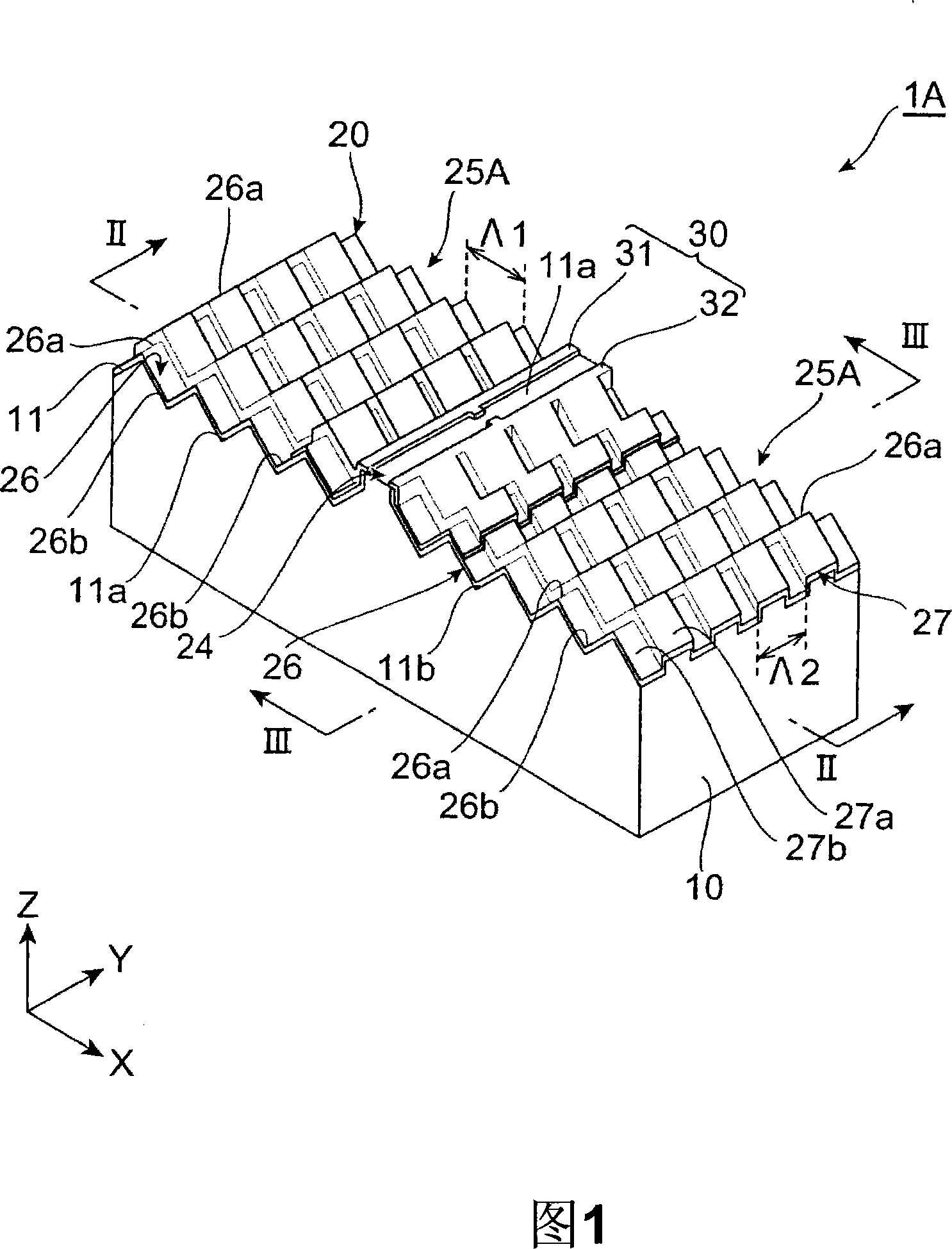
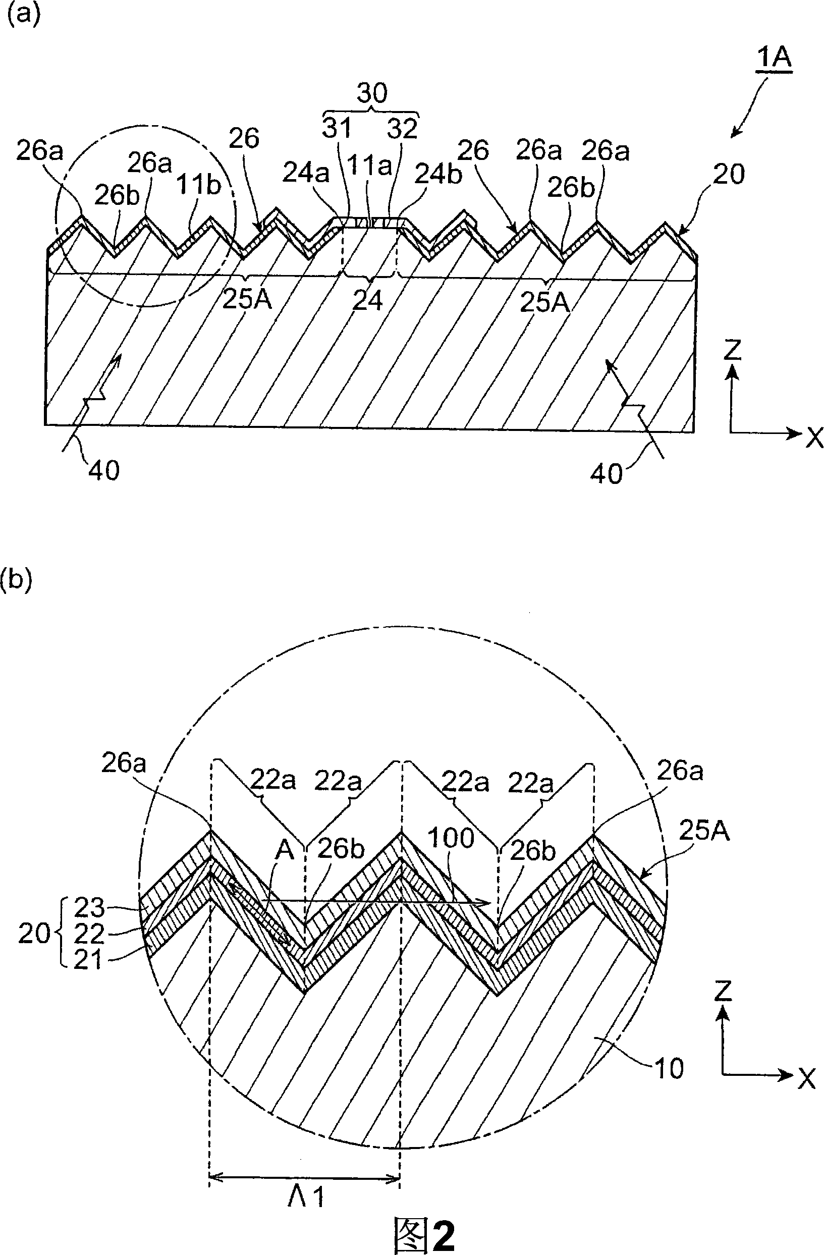
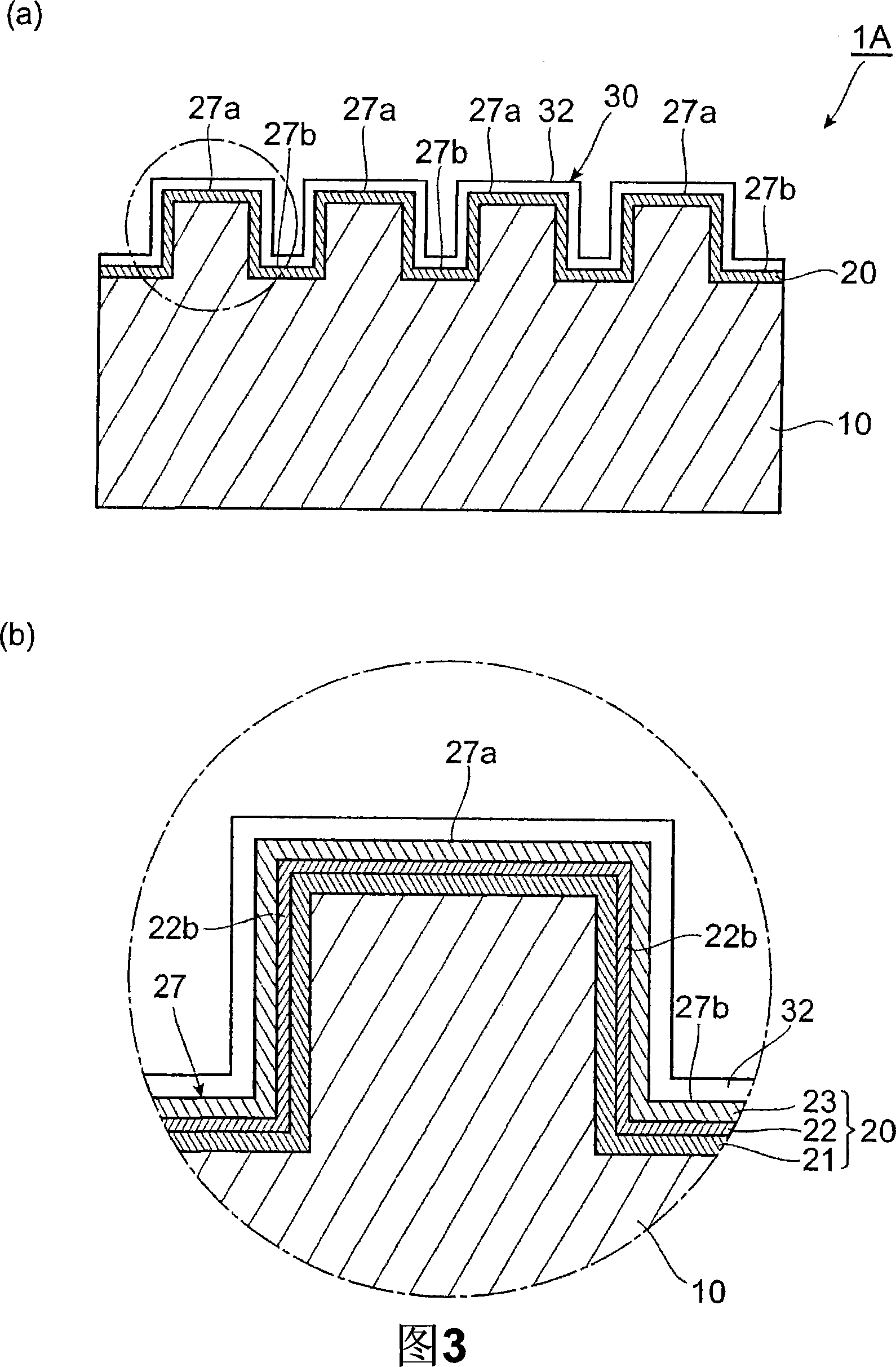
[0070] Fig. 1 is a perspective view of an embodiment of the optical element of the present invention. Fig. 2 is a cross-sectional view along the line II-II of Fig. 1 and an enlarged schematic view of a part thereof. Fig. 3 is a cross-sectional view along the line III-III of Fig. 1 and an enlarged schematic view of a part thereof. One embodiment of the waveguide structure of the present invention is used in the optical element 1A. The optical element 1A shown in Fig. 1 is used for detecting the wavelength of 30μm~1000μm (or the vibration frequency of 1.9×10 12 ~6.3×10 13 (1 / sec)) light is a THz wave light-receiving element of THz wave.
[0071]The optical element 1A has a semiconductor substrate 10 made of, for example, GaAs that can propagate THz waves, and a layered waveguide section 20 is laminated on the semiconductor substrate 10. In the following description, the lamination direction (arrangement direction) in which the waveguide portion 20 is laminated with respect to the se...
no. 2 Embodiment approach
[0117] Fig. 12 is a perspective view of a second embodiment of the optical element of the present invention. The main difference in structure between the optical element 1B and the optical element 1A is that the periodic structure portion 25B of the waveguide portion 20 has a concavo-convex pattern 26 in the X-axis direction, but does not have a concavo-convex pattern in the Y-axis direction. The optical element 1B will be described centering on this point.
[0118]In the waveguide portion 20 laminated on the semiconductor substrate 10 of the optical element 1B, an opening (light-concentrating portion) 24 is formed, and regions on both sides of the opening 24 are periodic structure portions 25B and 25B. Furthermore, the periodic structure part 25B has a concavo-convex pattern 26 which functions as a surface plasmon wave generator having a period Λ1.
[0119] The optical element 1B can be manufactured by the following method, for example. First, the steps shown in FIGS. 5 to 8 in t...
no. 3 Embodiment approach
[0122] Fig. 13 is a perspective view of a third embodiment of the optical element of the present invention. Fig. 14 is a cross-sectional view taken along the line XIV-XIV of Fig. 13.
[0123] The optical element 1C is a THz wave generating element that generates THz waves. The main difference in structure between the optical element 1C and the optical element 1B of the second embodiment is that in the optical element 1C, a semiconductor layer 50 is also laminated on the waveguide portion 20 laminated on the semiconductor substrate 10, and the semiconductor layer 50 is A THz wave generator 60 is provided on the surface 51. The optical element 1C will be described centering on this point. Here, the dashed-dotted lines in FIGS. 13 and 14 are schematic lines for explaining the boundary between the semiconductor substrate 10 and the semiconductor layer 50. In addition, in FIG. 13 and FIG. 14, in order to explain the structure of the waveguide section 20, the waveguide section 20 is sho...
PUM
 Abstract
Description
Claims
Application Information
 - Generate Ideas
- Intellectual Property
- Life Sciences
- Materials
- Tech Scout
- Unparalleled Data Quality
- Higher Quality Content
- 60% Fewer Hallucinations
Browse by: Latest US Patents, China's latest patents, Technical Efficacy Thesaurus, Application Domain, Technology Topic, Popular Technical Reports.
© 2025 PatSnap. All rights reserved.Legal|Privacy policy|Modern Slavery Act Transparency Statement|Sitemap|About US| Contact US: help@patsnap.com


