Photo-detector, space information detection device using the photo-detector, and photo-detection method
A photoelectric detector and photoelectric conversion technology, applied in the direction of optical devices, measuring devices, photometry, etc., can solve the problems that the signal light cannot extract a large amount of received light output, the dynamic range of the signal light is reduced, and the control is complicated.
- Summary
- Abstract
- Description
- Claims
- Application Information
AI Technical Summary
Problems solved by technology
Method used
Image
Examples
no. 1 example
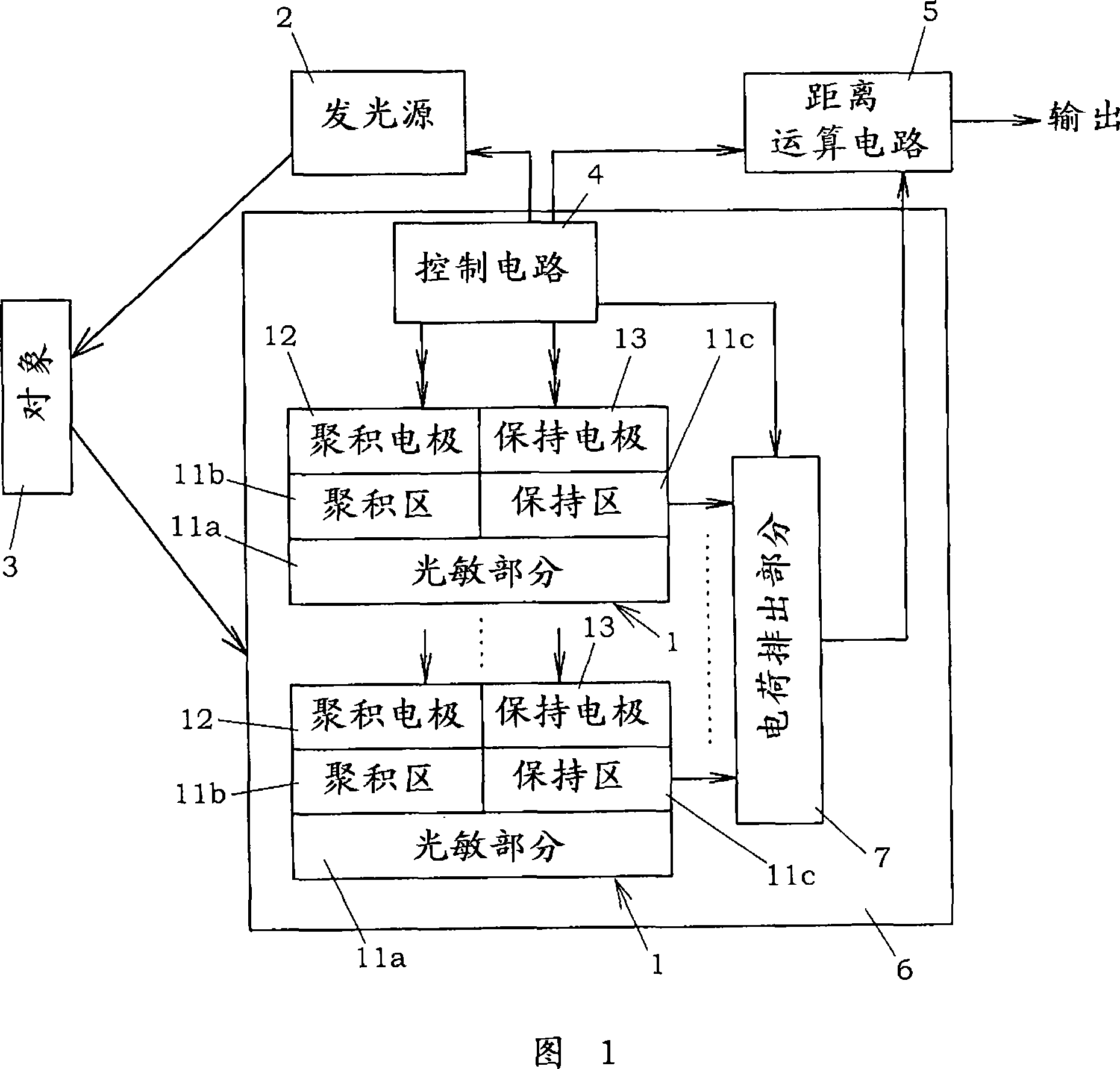
[0068] FIG. 1 shows a distance measuring device, which is a spatial information detection device using the photodetector 6 of this embodiment. In this distance measuring device, light is projected from a light emitting source 2 to a target space including an object 3 to be measured, and a photodetector 6 receives light including light reflected on the object from the target space, so as to obtain from the photodetector 6 a The received light output of the light quantity of reflected light. In order to measure the distance to the object by this configuration, a technique using the principle of triangulation, or a technique of measuring the flight time of light from the light emitting source 2 to the photodetector 6 is mainly utilized.
[0069] When the principle of triangulation is used, a parallel light beam of a predetermined pattern is projected from the light emitting source 2 to the target space, and the projected pattern on the target 3 is received by the photodetector 6 ...
no. 2 example
[0137] As shown in FIG. 6 , the present embodiment is characterized in that two accumulation electrodes ( 12 a , 12 b ) and two sustain electrodes ( 13 a , 13 b ) are formed for each of the photoelectric conversion portions 1 . That is, two accumulation electrodes (12a, 12b) and two sustain electrodes (13a, 13b) are defined as one group (or one pixel). Two sustaining electrodes (13a, 13b) are arranged spaced apart from each other. Two accumulating electrodes (12a, 12b) are arranged between the holding electrodes (13a, 13b). In addition, the accumulation electrodes (12a, 12b) are separated from each other by a gap "g", which is greater than the distance between each of the accumulation electrodes (12a, 12b) and the adjacent sustaining electrodes (13a, 13b). In this configuration, light is incident on the photosensitive portion 11a through the aperture between the light-shielding films 15 for covering the holding electrodes (13a, 13b). In addition, as shown in FIG. 7 , a light...
no. 3 example
[0169] In the second embodiment, since the gap "g" becomes wider, electrons and holes can be easily separated. In the case where the photodetector 6 is formed by arranging a plurality of photoelectric conversion parts 1 and the main functional layer 11 is also used as a vertical transfer transistor, since the accumulation electrodes (12a, 12b) and the holding electrodes (13a, 13b) ) and the potential well formed in the main functional layer 11 to transport carriers (electrons or holes), so there is a concern that when the gap "g" is excessively increased, the part for the gap "g" cannot be formed for Potential well for transporting charge carriers.
[0170] As shown in FIG. 9A, the present embodiment is characterized by forming a transfer electrode 22 between accumulation electrodes (12a, 12b). In this case, there is an advantage that electrons and holes are easily separated by increasing the distance between accumulation electrodes (12a, 12b), and also it is easy to transfer...
PUM
 Abstract
Description
Claims
Application Information
 - R&D
- Intellectual Property
- Life Sciences
- Materials
- Tech Scout
- Unparalleled Data Quality
- Higher Quality Content
- 60% Fewer Hallucinations
Browse by: Latest US Patents, China's latest patents, Technical Efficacy Thesaurus, Application Domain, Technology Topic, Popular Technical Reports.
© 2025 PatSnap. All rights reserved.Legal|Privacy policy|Modern Slavery Act Transparency Statement|Sitemap|About US| Contact US: help@patsnap.com


