Memory data protecting device and LSI for IC card
A data protection and storage technology, applied in memory systems, electrical digital data processing, instruments, etc., can solve problems such as illegal actions, cannot guarantee data security status, etc., and achieve the effect of reliable access control
- Summary
- Abstract
- Description
- Claims
- Application Information
AI Technical Summary
Problems solved by technology
Method used
Image
Examples
no. 1 example
[0034] FIG. 1 is a flowchart showing a schematic processing flow of a memory data protection method of a memory data protection device according to a first embodiment of the present invention.
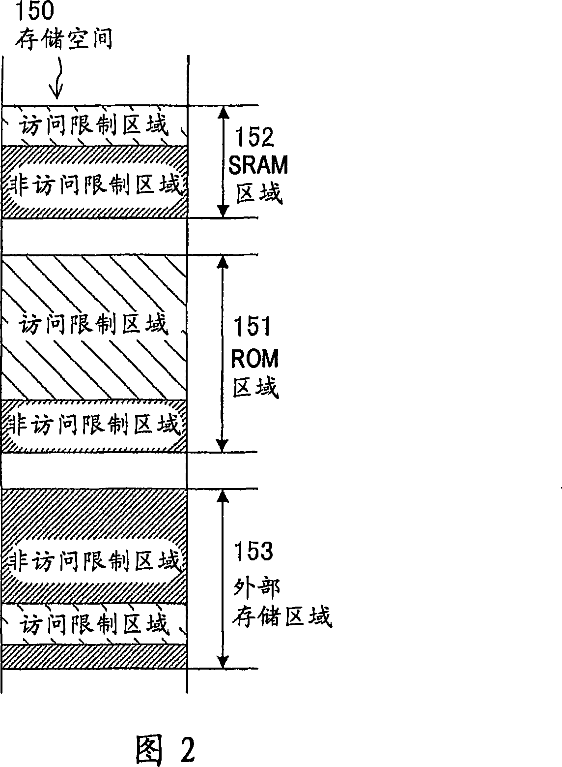
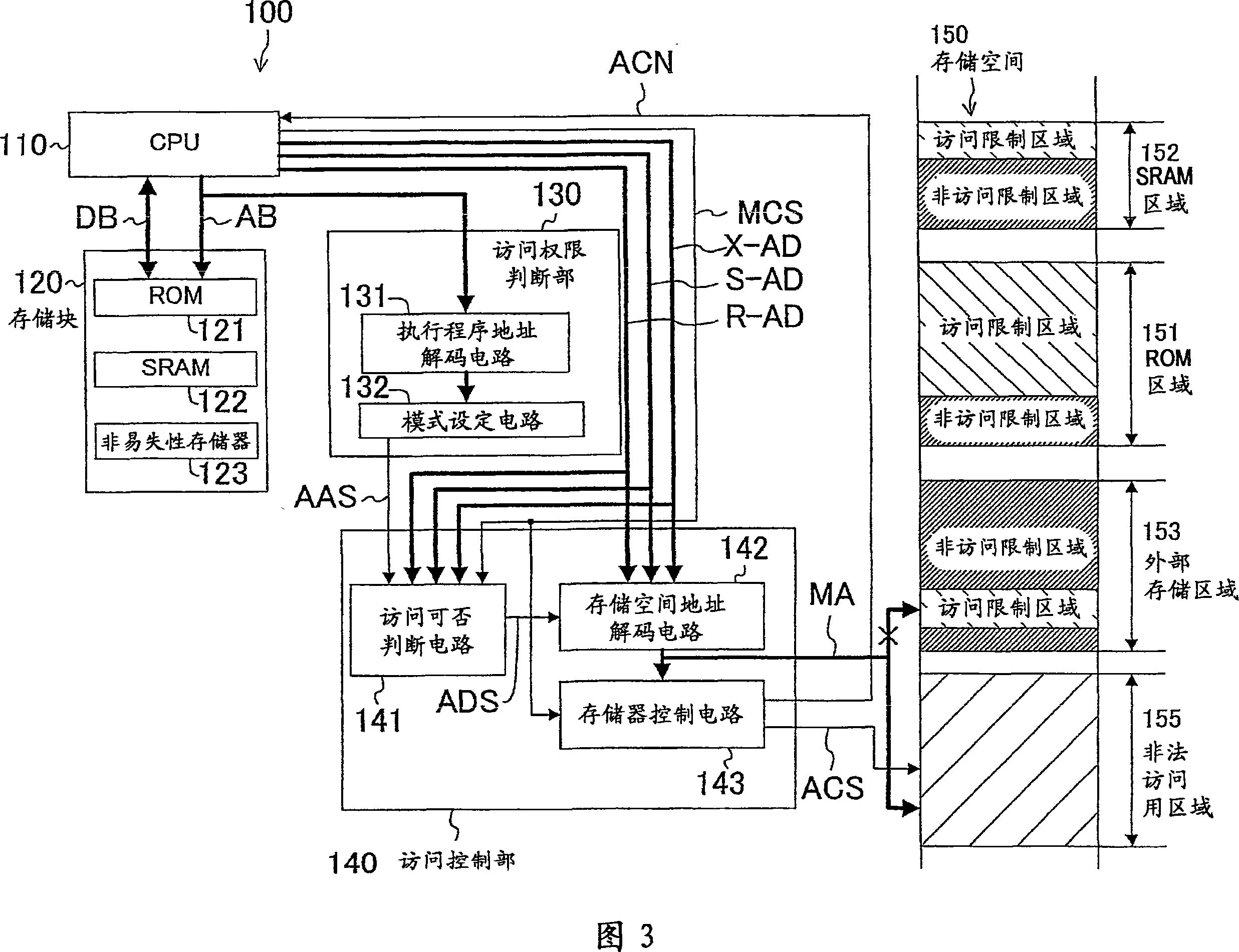
[0035] In the figure, when an execution program to be executed by the CPU accesses data in the memory (step S1), the access authority of the execution program to secure data in the memory is judged (step S2). Here, in the ROM of the memory data protection device of the present invention, API programs such as library files with access authority to the security data and OS programs such as application programs without the access authority are stored. In the above-mentioned step S2, it is judged Whether the execution program read by the CPU from the ROM is any one of the above-mentioned API program and the above-mentioned OS program, and judges the access authority.
[0036] According to the access authority of the above-mentioned execution program judged in the above-mentioned step S2 an...
no. 2 example
[0063] FIG. 4 is a block diagram showing the overall structure of a memory data protection device according to a second embodiment of the present invention.
[0064] The memory data protection device 200 of this embodiment differs from the memory data protection device 100 of the first embodiment shown in FIG. 3 only in that the storage space 150 has a register 250 for illegal access. The description of other structures is omitted since they are the same as those of the first embodiment.
[0065]A preset random number is stored in the illegal access register 250 provided in the storage space 150 . When the access permission judgment circuit 141 in the access control unit 140 judges that the access is illegal, the storage space address decoding circuit 142 changes the mapping of the logical address of the security data to be accessed by the execution program into the physical address assigned to the above-mentioned register 250 for illegal access. , and output the physical add...
no. 3 example
[0071] FIG. 5 is a block diagram showing the overall structure of a memory data protection device according to a third embodiment of the present invention.
[0072] The only difference between the memory data protection device 300 of this embodiment and the memory data protection device 100 of the first embodiment shown in FIG. As for other structures, since they are the same as the memory data protection device of the first embodiment, their descriptions are omitted.
[0073] When the access permission judging circuit 141 in the access control unit 140 determines that the access is illegal, the storage space address decoding circuit 142 transmits the logical address of the secure data to be accessed by the program execution to the memory control circuit 350 .
[0074] When the access to the safety data of the above-mentioned execution program is a write processing access, according to the memory control signal MCS input from the CPU 11 and the memory of the logical address of...
PUM
 Abstract
Description
Claims
Application Information
 - Generate Ideas
- Intellectual Property
- Life Sciences
- Materials
- Tech Scout
- Unparalleled Data Quality
- Higher Quality Content
- 60% Fewer Hallucinations
Browse by: Latest US Patents, China's latest patents, Technical Efficacy Thesaurus, Application Domain, Technology Topic, Popular Technical Reports.
© 2025 PatSnap. All rights reserved.Legal|Privacy policy|Modern Slavery Act Transparency Statement|Sitemap|About US| Contact US: help@patsnap.com


