Method for manufacturing semiconductor package structure having micro electro-mechanical system

A micro-electro-mechanical system and packaging structure technology, which is applied in semiconductor/solid-state device manufacturing, microstructure technology, semiconductor devices, etc., can solve problems such as high difficulty and increased production costs, and achieve reduced production costs, increased production, and application broad effect

Active Publication Date: 2010-10-13
ADVANCED SEMICON ENG INC
View PDF3 Cites 0 Cited by
  • Summary
  • Abstract
  • Description
  • Claims
  • Application Information

AI Technical Summary

Problems solved by technology

Furthermore, if photolithography is used to remove these connecting portions 132, it will be more difficult and will increase the production cost.

Method used


Image

  • Method for manufacturing semiconductor package structure having micro electro-mechanical system
  • Method for manufacturing semiconductor package structure having micro electro-mechanical system
  • Method for manufacturing semiconductor package structure having micro electro-mechanical system

Examples


Embodiment Construction

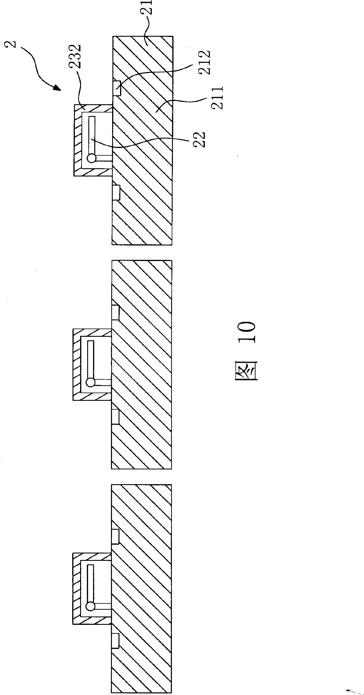
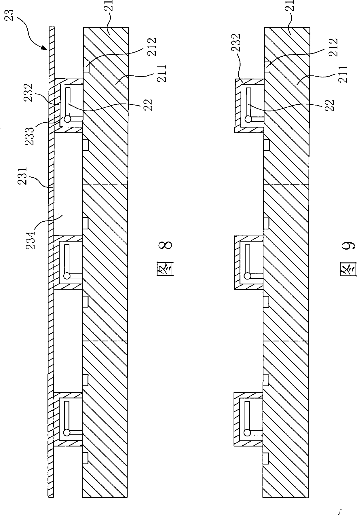
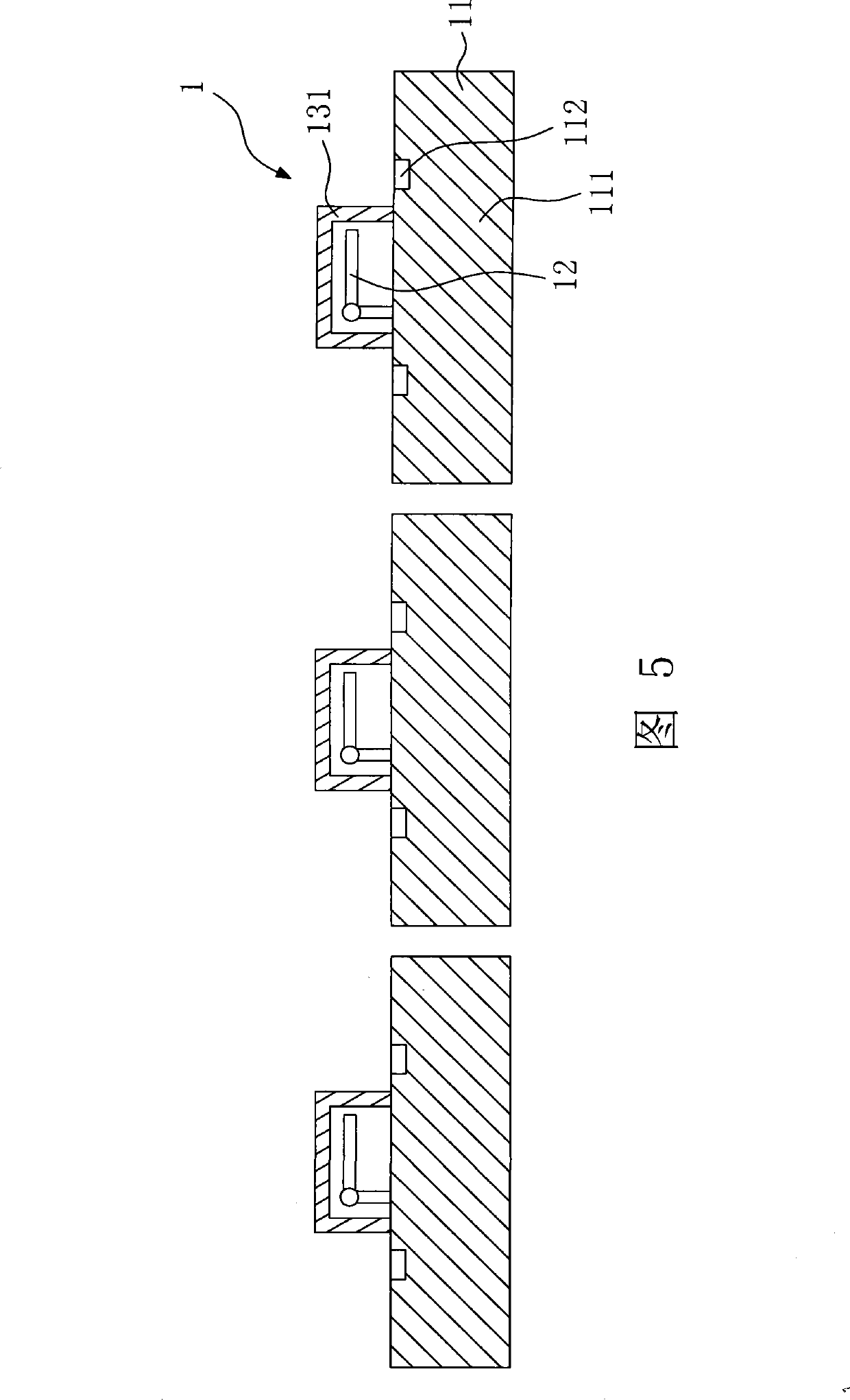
[0018] Refer to Figure 6 to Figure 10 , which shows a schematic diagram of the manufacturing method of the semiconductor package structure with Micro-Electro-Mechanical Systems (MEMS) of the present invention. first reference Image 6, A substrate 21 is provided, and the substrate 21 has a plurality of substrate units 211 (shown by dotted lines), and each substrate unit 211 has a plurality of pads 212 . The substrate 21 can be a CMOS wafer.

[0019] refer to Figure 7 , disposing a MEMS 22 on each substrate unit 211 . In this embodiment, the MEMS 22 is an optical element. The MEMS 22 includes at least one microlens set 221 , and each of the microlens sets 221 includes: a support member 222 , a hinge 223 and a microlens 224 . The support member 222 has a first end 225 and a second end 226 , wherein the second end 226 of the support member 222 is located on the substrate unit 211 . The hinge 223 is disposed on the first end 225 of the support member 222 . One end of the ...


PUM


Abstract

The process of manufacturing semiconductor package structure with micro electromechanical system includes the following steps: setting several micro electromechanical systems onto base plate units in one base plate, sealing these micro electromechanical systems with several covering bodies of one cover plate, eliminating the main body of the cover plate, and cutting the base plate to form severalsemiconductor package structures. The process has no need of forming locating markers and is simple. In addition, the cover plate has no need of being made of transparent material and the main body may be eliminated through a simple grinding step, so that the present invention has wide application and low production cost.

Description

technical field [0001] The present invention relates to a manufacturing method of a semiconductor packaging structure, and in particular to a manufacturing method of a semiconductor packaging structure with a micro-electromechanical system. Background technique [0002] Please refer to Figure 1 to Figure 5 , which shows a schematic diagram of a conventional manufacturing method of a semiconductor package structure with micro-electro-mechanical systems (Micro-Electro-Mechanical Systems, MEMS). Please refer to figure 1, Firstly, a substrate 11 is provided. The substrate 11 has a plurality of substrate units 111 (shown by dotted lines), and each substrate unit 111 has a plurality of pads 112 . [0003] Please refer to figure 2 , setting a plurality of MEMS 12 on each substrate unit 111 . Referring to FIG. 3 , a cover plate 13 is provided, and the cover plate 13 has a plurality of covers 131 and a plurality of connecting portions 132 , and the connecting portions 132 conne...

Claims


Application Information

Patent Timeline
Patent Type & Authority Patents(China)
IPC IPC(8): B81C3/00H01L21/50
CPCH01L2924/16235
Inventor 王盟仁
Owner ADVANCED SEMICON ENG INC
Why Eureka
Try Eureka