Flat board display of splayed inclined bar control structure and its making process

A flat-panel display and manufacturing process technology, which is applied in the field of flat-panel display technology, and can solve the problems of large gate current and high gate voltage, etc.

Inactive Publication Date: 2007-11-28
ZHONGYUAN ENGINEERING COLLEGE
View PDF0 Cites 14 Cited by
  • Summary
  • Abstract
  • Description
  • Claims
  • Application Information

AI Technical Summary

Problems solved by technology

[0003] Among field emission display devices with a three-electrode structure, most displays currently adopt a structural mode in which the gate structure is located above the carbon nanotube cathode structure. The manufacturing process is simple and the gate control function is significant, but the gate current is relatively large. , the gate voltage remains high, which is the disadvantage of

Method used


Image

  • Flat board display of splayed inclined bar control structure and its making process
  • Flat board display of splayed inclined bar control structure and its making process
  • Flat board display of splayed inclined bar control structure and its making process

Examples


Embodiment Construction

[0039] The present invention will be further described below with reference to the drawings and embodiments, but not limited to these embodiments.

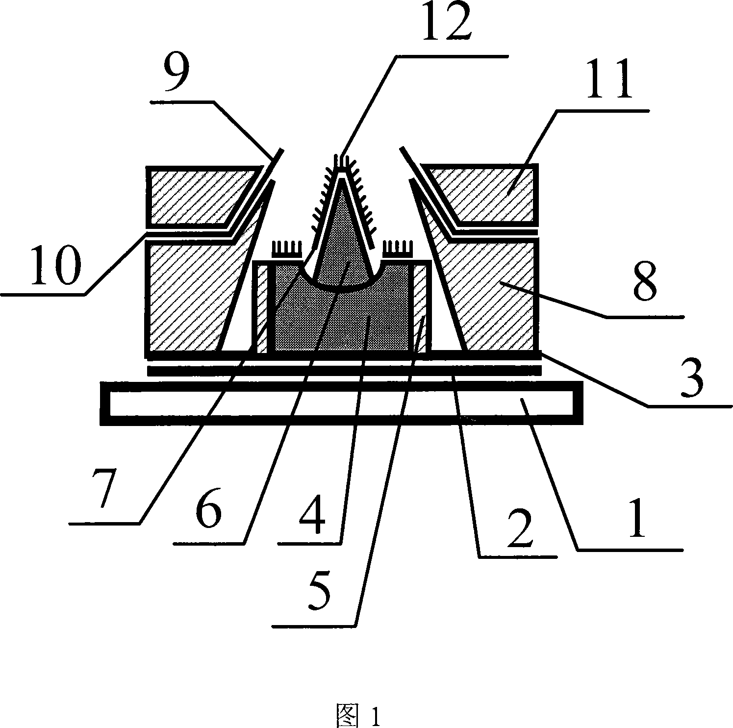
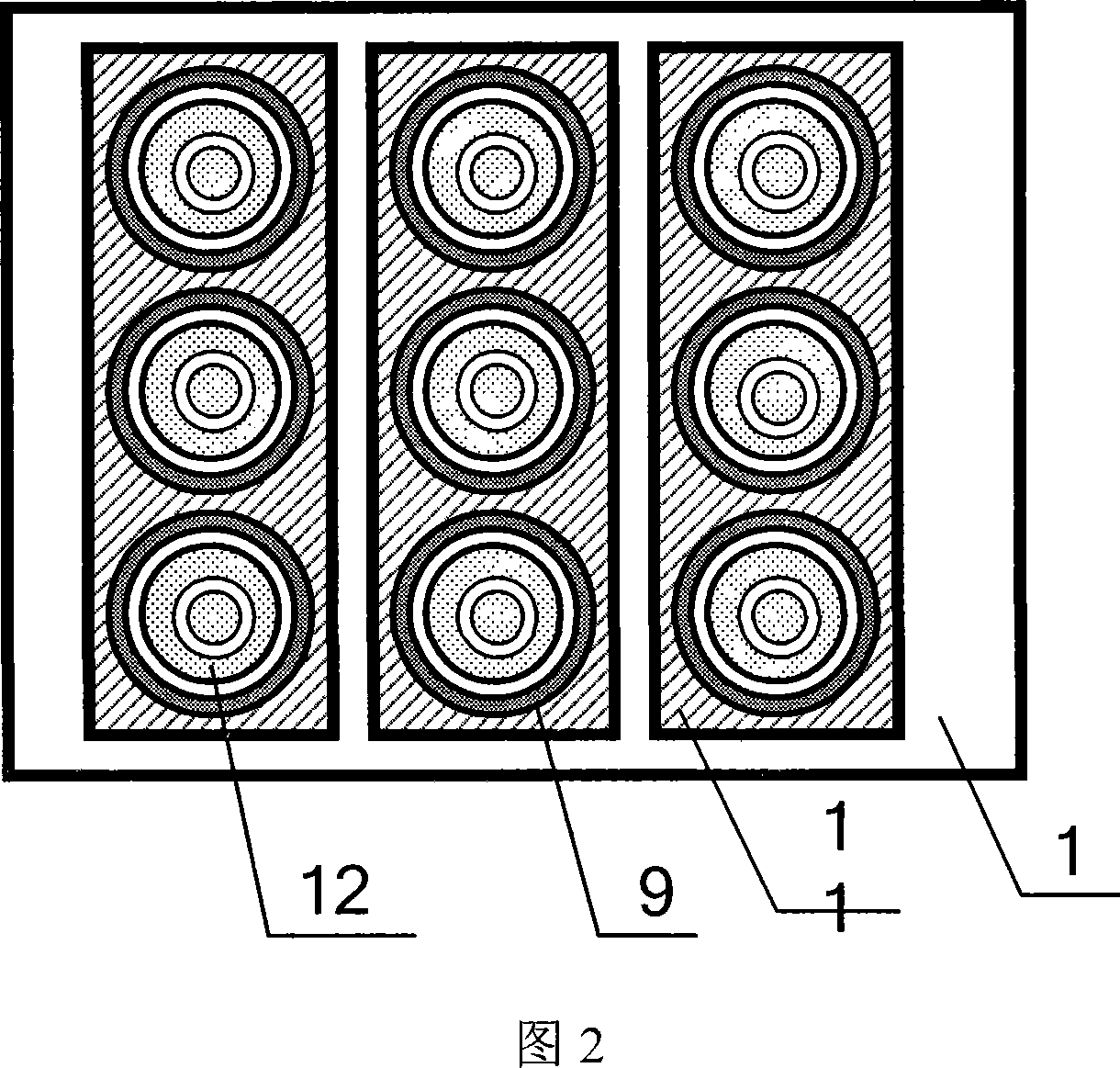
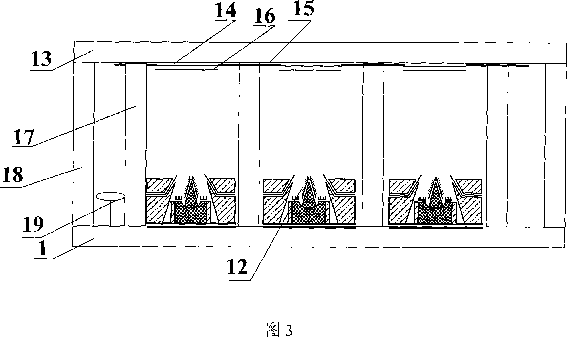
[0040] The flat-panel display with a figure-eight oblique grid control structure includes a sealed vacuum chamber formed by an anode glass panel [13], a cathode glass panel [1] and surrounding glass frames [18]; The panel has an anode conductive layer [14] and a phosphor layer [16] prepared on the anode conductive layer; on the cathode glass panel, there are grid lead layers [10], carbon nanotubes [12] and figure-eight slanted grid control structure; support wall structure [17] and getter [19] accessory elements located between the anode glass panel and the cathode glass panel.

[0041] The eight-shaped oblique grid control structure includes a cathode glass panel [1], a retardation layer [2], a cathode lead layer [3], a lifting layer [4], a cathode covering layer [5], and a lifting layer [6] ], cathode conductive layer [7], spac...


PUM


Abstract

This invention relates to a flat display of slant grid-control structure and its manufacturing method including a closed vacuum cavity composed of an anode glass panel, a cathode glass panel and glass frame around it, in which, an anode conductive layer is set on the anode glass panel and a fluorescent powder layer is prepared on the anode conductive layer, a supporting wall structure and attached elements of a getter is set between the anode glass panel and the cathode glass panel, a grid lead layer, carbon nanometer tubes and a slant grid-control structure are set on the cathode glass panel to control efficiency of the grid structure and increase the electronic emission efficiency and quantity to increase image quality of the device.

Description

technical field [0001] The invention belongs to the fields of flat panel display technology, microelectronic science and technology, vacuum science and technology, and nano science and technology, and relates to device fabrication of flat panel field emission displays, in particular to carbon nanotube cathodes. The device manufacturing aspect of the flat field emission display, especially relates to a flat panel display with a figure-eight oblique grid control structure and its manufacturing process. Background technique [0002] In recent years, flat panel display technology has been greatly developed. Driven by high-definition televisions, computer monitors, automotive terminal display equipment, and military helmet visors, display technology is moving towards high-resolution, low-efficiency Voltage, planarization, and large-scale development. Field emission display is a light-emitting device made by applying vacuum microelectronics technology to display equipment. It has...

Claims


Application Information

Patent Timeline
IPC IPC(8): H05B33/26H05B33/14H05B33/10G09F9/00
Inventor 李玉魁
Owner ZHONGYUAN ENGINEERING COLLEGE
Why Eureka
Try Eureka