
Single-end input and dual-end output amplifier circuit and signal processing circuit

A signal processing circuit and amplifier circuit technology, which is applied in the direction of improving amplifiers to reduce noise effects, etc., can solve problems such as double-ended output signal quality effects, and achieve the effects of saving external parts, good circuit performance, and low-cost circuit design.

Inactive Publication Date: 2007-11-28
PRINCETON TECHNOLOGY
View PDF0 Cites 9 Cited by
  • Summary
  • Abstract
  • Description
  • Claims
  • Application Information

AI Technical Summary

Problems solved by technology

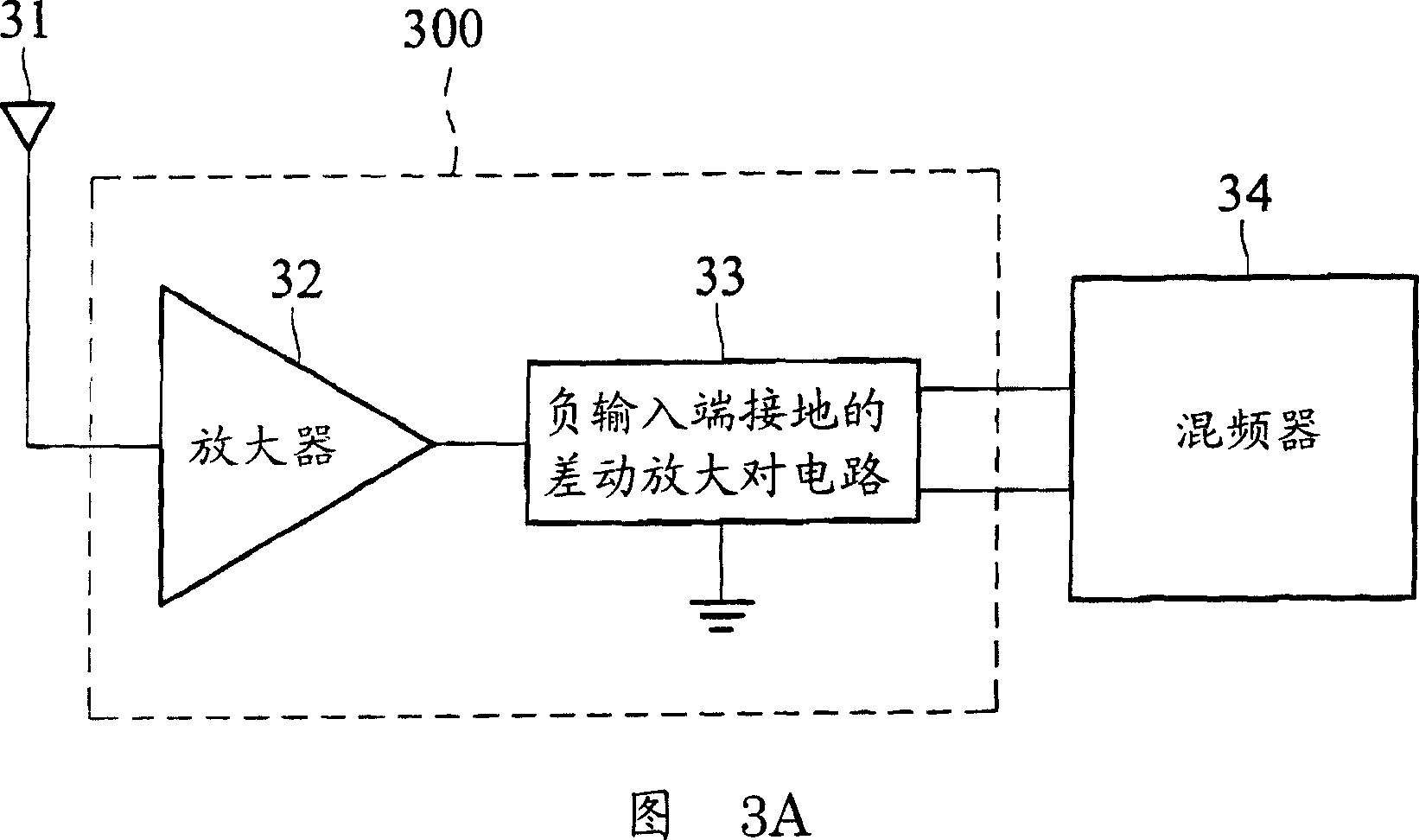
[0009] However, although the method of replacing the single-ended to double-ended conversion circuit 23 with the traditional differential amplifier pair circuit 33 with the negative input terminal grounded reduces the chip area, due to the bypass of the differential amplifier circuit 33 with the traditional negative input terminal grounded The (bypass) capacitor 306 will couple the noise on the chip to the input end of the differential amplifier pair circuit 33 whose negative input end is grounded, so the quality of the double-ended output signal at the output end of the amplifier circuit 300 will be affected by the noise.

Method used


Image

  • Single-end input and dual-end output amplifier circuit and signal processing circuit
  • Single-end input and dual-end output amplifier circuit and signal processing circuit
  • Single-end input and dual-end output amplifier circuit and signal processing circuit

Examples


Embodiment Construction

[0047] In order to make the above-mentioned purposes, features and advantages of the present invention more obvious and understandable, a preferred embodiment is specifically cited below, and in conjunction with the accompanying drawings, the detailed description is as follows:

[0048] 4A is a circuit diagram showing a single-ended input and double-ended output amplifier 400 according to an embodiment of the present invention, including a single-ended input single-ended output amplifier (Amplifier) ​​42 and a single-ended to double-ended converter 43 . The antenna 41 is coupled to the input of a single-ended input single-ended output amplifier 42 , and the output terminal of the single-ended input single-ended output amplifier 42 is coupled to the input terminal of a single-ended to double-ended converter 43 . The single-ended input and double-ended output amplifier 400 in FIG. 4A further includes a first capacitor 45 coupled between the single-ended input and single-ended out...


PUM


Abstract

The invention discloses a single-end input double-end output amplifier circuit and signal disposing circuit, which comprises the following parts: amplifier to amplify the input signal, input end to receive the input signal and first output end, single-end input double-end output conversion circuit to converse the amplified signal to differential signal, first transistor to receive the amplified signal, first grid to couple the first output end, first first pole to couple the second output end, first second pole to couple the first node, second transistor with second grid to couple the second first pole of third output end, second second pole to couple the first node, second capacitance coupled between the second output end and second grid, first resistance coupled between the second output end and power source, second resistance coupled between the third output end and voltage source, current source coupled between the first node and ground point.

Description

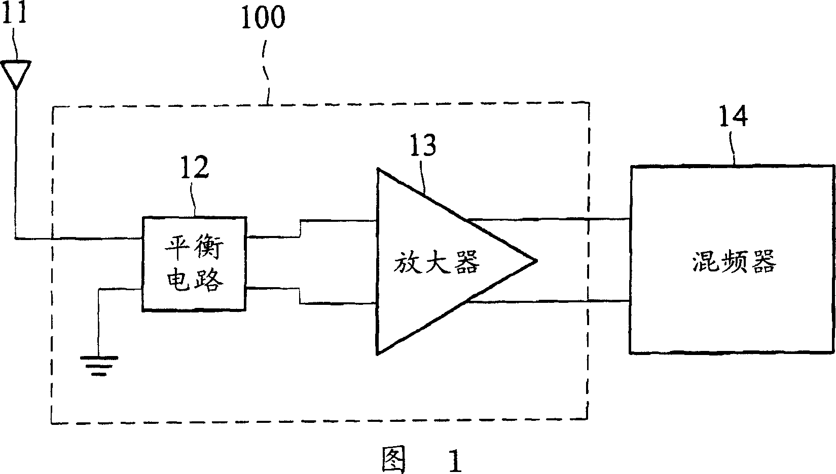
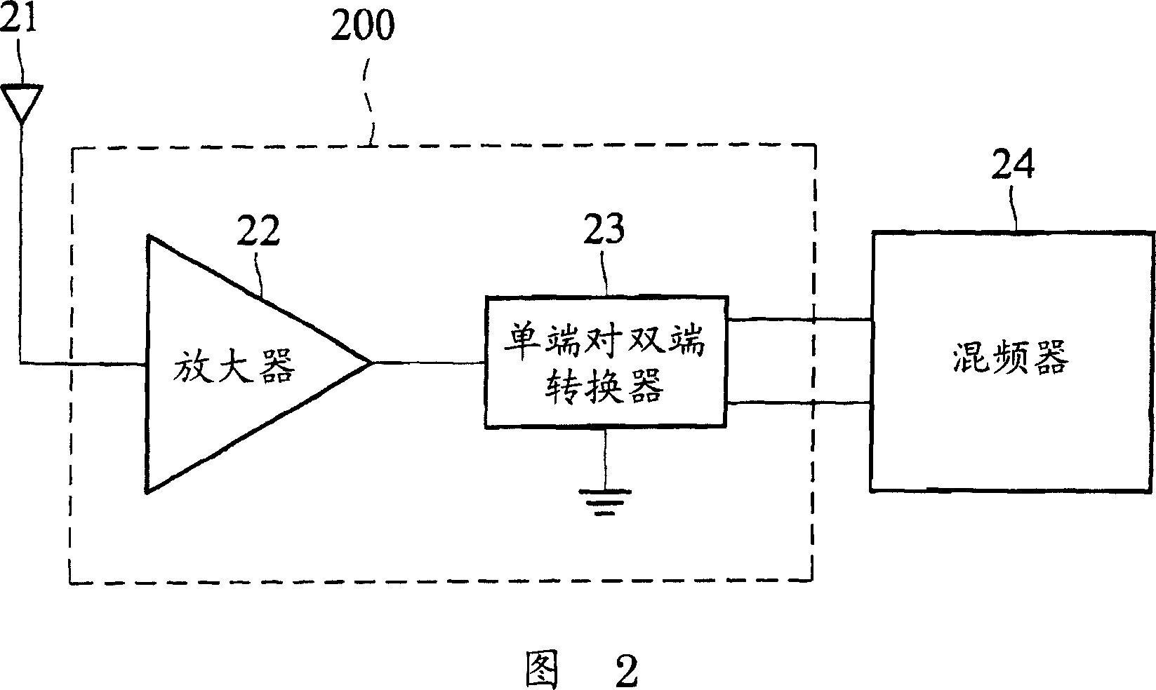
technical field [0001] The invention relates to a signal processing circuit, in particular to a low noise amplifier circuit with single-end input and double-end output. Background technique [0002] Most of the antennas currently used are single-ended antennas, but the Image-rejection Mixer (Image-rejection Mixer) used to down-frequency the signal usually uses a Double-Balanced Mixer (Double-Balanced Mixer) with double-ended input. Mixer) to achieve. Therefore, the single-ended input signal received by the antenna must be converted to a double-ended output signal before the image signal cancellation mixer can down-convert the signal from the antenna side for back-end processing. [0003] There are currently two methods for converting a single-ended input signal into a double-ended output signal. FIG. 1 shows one single-ended input and double-ended output amplifier circuit 100 , including a balancing circuit (Balun) 12 and a double-ended input and double-ended output amplif...

Claims


Application Information

Patent Timeline
IPC IPC(8): H03F1/26
Inventor 高念安张国威
Owner PRINCETON TECHNOLOGY
Learn More