
Semiconductor device having a frontside contact and vertical trench isolation and method of fabricating same

A semiconductor and trench technology, used in semiconductor/solid-state device manufacturing, semiconductor devices, electric solid-state devices, etc., can solve problems such as interfering with the performance of adjacent devices

Inactive Publication Date: 2007-09-19
NXP BV
View PDF1 Cites 9 Cited by
  • Summary
  • Abstract
  • Description
  • Claims
  • Application Information

AI Technical Summary

Problems solved by technology

Said crosstalk occurs as a result of applied voltages in active devices causing potential fluctuations through horizontal dielectric isolation; thus disturbing the performance of adjacent devices

Method used


Image

  • Semiconductor device having a frontside contact and vertical trench isolation and method of fabricating same
  • Semiconductor device having a frontside contact and vertical trench isolation and method of fabricating same
  • Semiconductor device having a frontside contact and vertical trench isolation and method of fabricating same

Examples


Embodiment Construction

[0035] Referring to FIG. 4 , FIGS. 4 a - 4 f and FIG. 5 , the method for fabricating a device according to an exemplary embodiment of the present invention will be described in detail below.

[0036] step 100

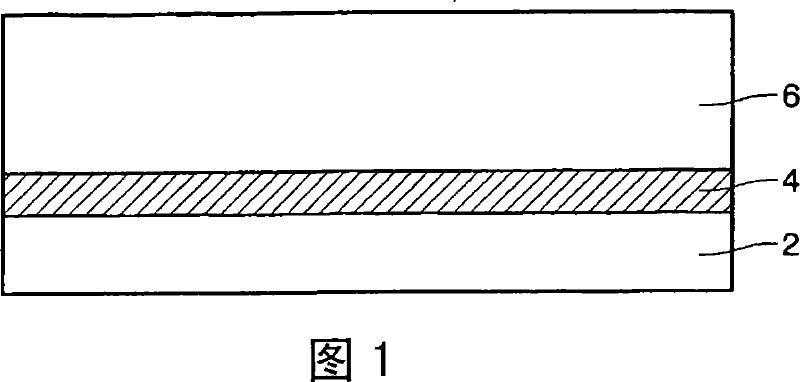
[0037] Consider a silicon-on-insulator substrate 20 as shown in FIG. 4, wherein the bottom substrate layer 2 is composed of silicon, and the insulating layer 4 is composed of silicon dioxide (SiO 2 ) composition, and the active semiconductor layer 6 is composed of silicon. In the first step, a field-induced oxide layer is grown on the exposed surface of the active semiconductor layer 6 of the substrate 20 by an oxidation process, the layer comprising silicon dioxide (SiO 2) layer 22, the oxidation process is well known to those of ordinary skill in the art. The purpose of the field oxide layer is to protect the active layer 6 of the substrate 20 and to form doped carriers. A subsequent nitridation step may also be performed to form a nitride (Si 3 N 4 ) layer 24. ...


PUM


Abstract

A method of forming a contact post (36) and surrounding isolation trench (28) in a semiconductor-on-insulator (SOI) substrate (20). The method comprises etching a contact hole (26) and surrounding isolation trench (28) from an active layer (6) of the substrate (20) to the insulating layer (4), masking the trench (28) and further etching the contact hole (26) to the base substrate layer (2), filling the trench (28) and contact hole (26) with undoped intrinsic polysilicon (34) and then performing a doping process in respect of the polysilicon material filling the contact hole (26) so as to form in situ a highly doped contact post (36), while the material filling the isolation trench (28) remains non-conductive. The method enables the isolation trench and contact post to be formed substantially simultaneously so as to avoid undue interference with the device fabrication process.

Description

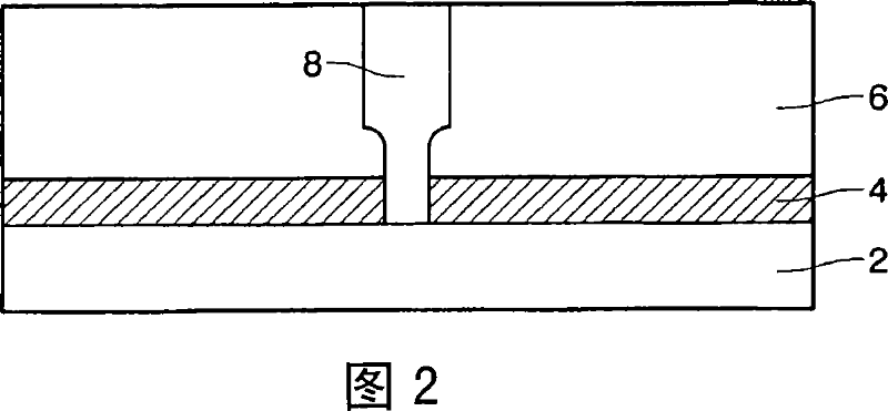
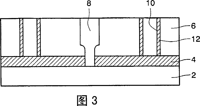
technical field [0001] In general, the present invention relates to semiconductor devices with front-side contacts and vertical trench isolation, and in particular, the present invention relates to an active semiconductor device with respect to a semiconductor-on-insulator (SOI-semiconductor-on-insulator) substrate Areas form contact pillars and separate trenches. Background technique [0002] Often, especially in high voltage applications, it is desirable to completely electrically isolate active semiconductor devices from the underlying semiconductor substrate ("vertical" isolation) and adjacent active devices ("horizontal" isolation). [0003] Vertical isolation of active devices is generally achieved by using a semiconductor-on-insulator (SOI) substrate. Referring to the SOI substrate shown in FIG. A buried insulator (usually silicon oxide) layer 4 formed on it; and an active bonding semiconductor (usually silicon) layer 6 formed on the buried insulator layer 4 . In th...

Claims


Application Information

Patent Timeline
Patent Type & Authority Applications(China)
IPC IPC(8): H01L21/74H01L27/12
CPCH01L21/76283H01L21/84H01L27/1203H01L21/743H01L21/74H01L21/20H01L27/12
Inventor 沃尔夫岗·劳舍尔
Owner NXP BV
Learn More