Magnetic-bias ferromagnetic spiral inductor

A technology of spiral inductors and inductors, applied in the direction of magnetic bias transformers, inductors, printed inductors, etc., can solve problems such as ohmic loss

Active Publication Date: 2011-07-06
TAIWAN SEMICON MFG CO LTD
View PDF0 Cites 0 Cited by
  • Summary
  • Abstract
  • Description
  • Claims
  • Application Information

AI Technical Summary

Problems solved by technology

However, this ideal inductor only exists in theory, and the actual inductor will have some ohmic loss (ohmicloss) and reactance

Method used


Image

  • Magnetic-bias ferromagnetic spiral inductor
  • Magnetic-bias ferromagnetic spiral inductor
  • Magnetic-bias ferromagnetic spiral inductor

Examples


Embodiment Construction

[0058] In order to further explain the technical means and effects that the present invention adopts to achieve the intended purpose of the invention, the specific implementation, structure, Features and their functions are described in detail below.

[0059] The following descriptions are only about examples of preferred embodiments of the present invention, and are not intended to limit the present invention and its application and use.

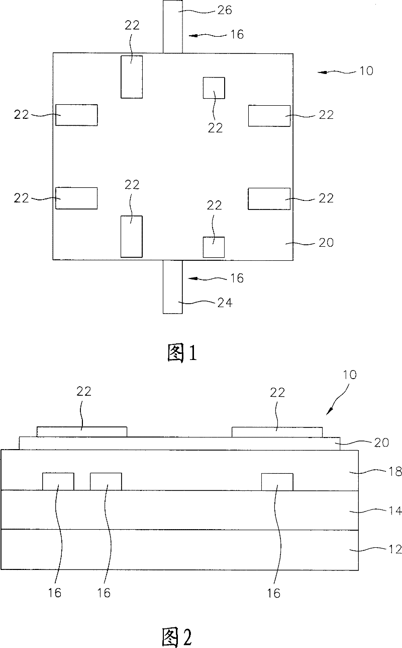
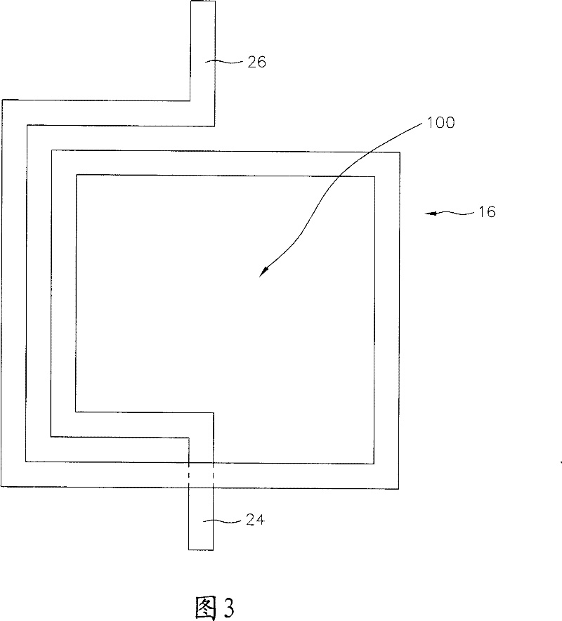
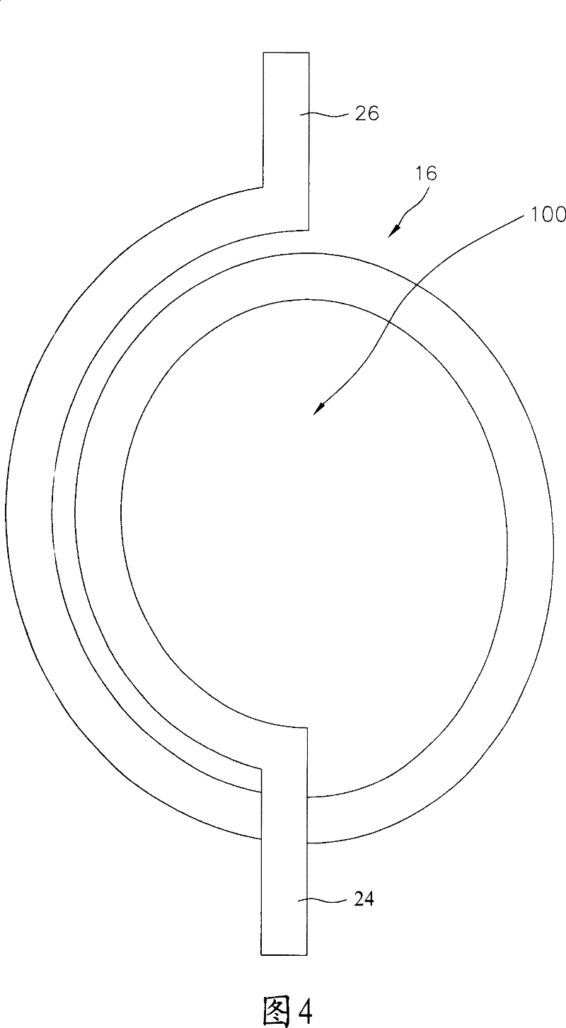
[0060] Please refer to figure 1 and figure 2 , an embodiment of the present invention includes a semiconductor device 10 including a semiconductor substrate 12 . Any semiconductor substrate 12 known to those skilled in the art may be utilized and may include, but is not limited to, silicon (silicon), germanium (Ge), indium (In), gallium (Ga), arsenic (As) and tin (Sn). The substrate 12 can be doped with various dopants including boron and phosphorous to define individual electronic components therein. A first insulating layer 14 is di...


PUM


Abstract

A semiconductor device having a semiconductor substrate and a first insulator overlying the semiconductor substrate. A spiral coil inductor overlies the first insulator and a second insulator overlies the spiral coil inductor. A patterned ferromagnetic film overlies the second insulator and a patterned magnetic-bias film overlies the patterned ferromagnetic film.

Description

technical field [0001] The present invention relates to a semiconductor device including an inductor, and more particularly to a magnetically biased ferromagnetic spiral inductor. Background technique [0002] An inductor is a device that stores energy in the form of a magnetic field. An inductor is also an electronic component that is specially designed to provide a controlled amount of inductance. Inductors usually include a long wire, which is wound into a spiral or ring shape, and the inductance of the inductor can be increased by placing a high-permeability core (core) in it value. Suitable materials such as iron, iron powder and magnetic materials may be used. Industrially used inductors have inductance values ​​ranging from less than 1 microHenry (μH) to about 10 Henry (H). Small inductors have been used in RF tuned circuits (tuned circuits) and RF chokes (chokes). Larger inductors have been used at audio frequencies with the largest inductance as filter chokes f...

Claims


Application Information

Patent Timeline
Patent Type & Authority Patents(China)
IPC IPC(8): H01F17/00
CPCH01F41/34H01F17/0006H01F3/10H01F19/08H01F2017/0086H01F2017/0066
Inventor 连万益邓端理林文钦王昭雄
Owner TAIWAN SEMICON MFG CO LTD
Why Eureka
Try Eureka